National Institute for R&D in Microtechnologies 126A, Erou Iancu Nicolae, 077190, Bucharest, Romania Tel: +40 21 269 07 78 Fax: +40 21 269 07 72 www.imt.ro - www.imt.ro/MINAFAB Research Centre for Integrated Systems Nanotechnologies and Carbon Based Nanomaterials CENASIC Programul Operaţional Sectorial „Creşterea Competitivităţii Economice“ „Investiţii pentru viitorul dumneavoastră“ CENTRUL DE CERCETARE PENTRU NANOTEHNOLOGII DEDICATE SISTEMELOR INTEGRATE ŞI NANOMATERIALE AVANSATE PE BAZĂ DE CARBON – CENASIC Proiect co-finanţat prin Fondul European de Dezvoltare Regională
Transcript
National Institute for R&D in Microtechnologies126A, Erou Iancu Nicolae, 077190, Bucharest, RomaniaTel: +40 21 269 07 78Fax: +40 21 269 07 72www.imt.ro - www.imt.ro/MINAFAB
Research Centre for Integrated Systems Nanotechnologies and Carbon Based Nanomaterials
CENASIC
Programul Operaţional Sectorial „Creşterea Competitivităţii Economice“„Investiţii pentru viitorul dumneavoastră“
CENTRUL DE CERCETARE PENTRU NANOTEHNOLOGII DEDICATE SISTEMELOR INTEGRATE ŞI NANOMATERIALE AVANSATE PE BAZĂ DE CARBON – CENASICProiect co-finanţat prin Fondul European de Dezvoltare Regională
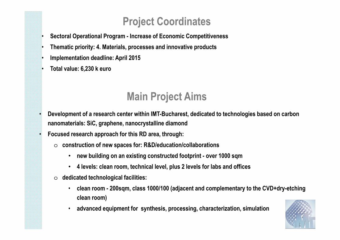
• Sectoral Operational Program - Increase of Economic Competitiveness• Thematic priority: 4. Materials, processes and innovative products• Implementation deadline: April 2015• Total value: 6,230 k euro
Project Coordinates
Main Project Aims• Development of a research center within IMT-Bucharest, dedicated to technologies based on carbon
nanomaterials: SiC, graphene, nanocrystalline diamond• Focused research approach for this RD area, through:
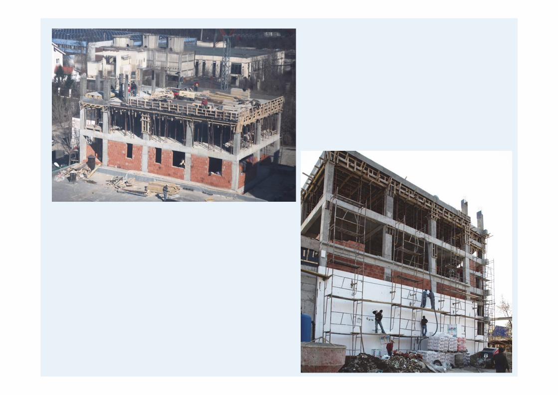
o construction of new spaces for: R&D/education/collaborations• new building on an existing constructed footprint - over 1000 sqm• 4 levels: clean room, technical level, plus 2 levels for labs and offices
o dedicated technological facilities: • clean room - 200sqm, class 1000/100 (adjacent and complementary to the CVD+dry-etching
clean room)• advanced equipment for synthesis, processing, characterization, simulation
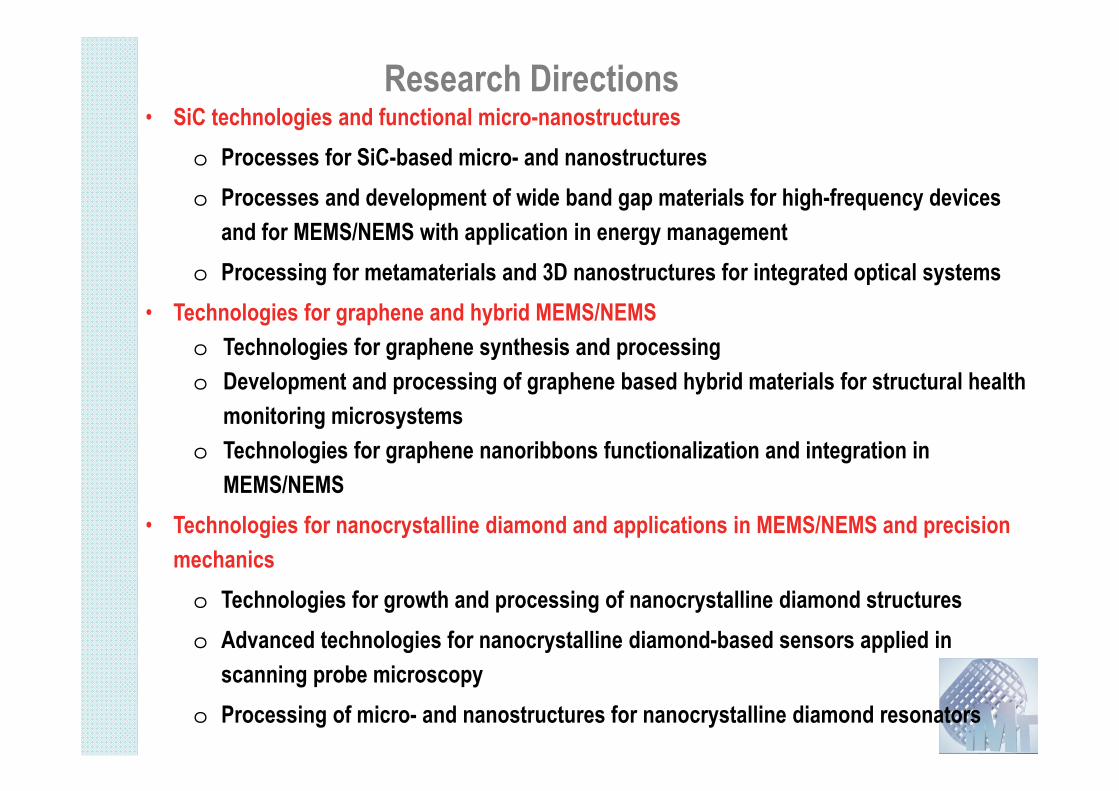
• SiC technologies and functional micro-nanostructureso Processes for SiC-based micro- and nanostructureso Processes and development of wide band gap materials for high-frequency devices
and for MEMS/NEMS with application in energy managemento Processing for metamaterials and 3D nanostructures for integrated optical systems
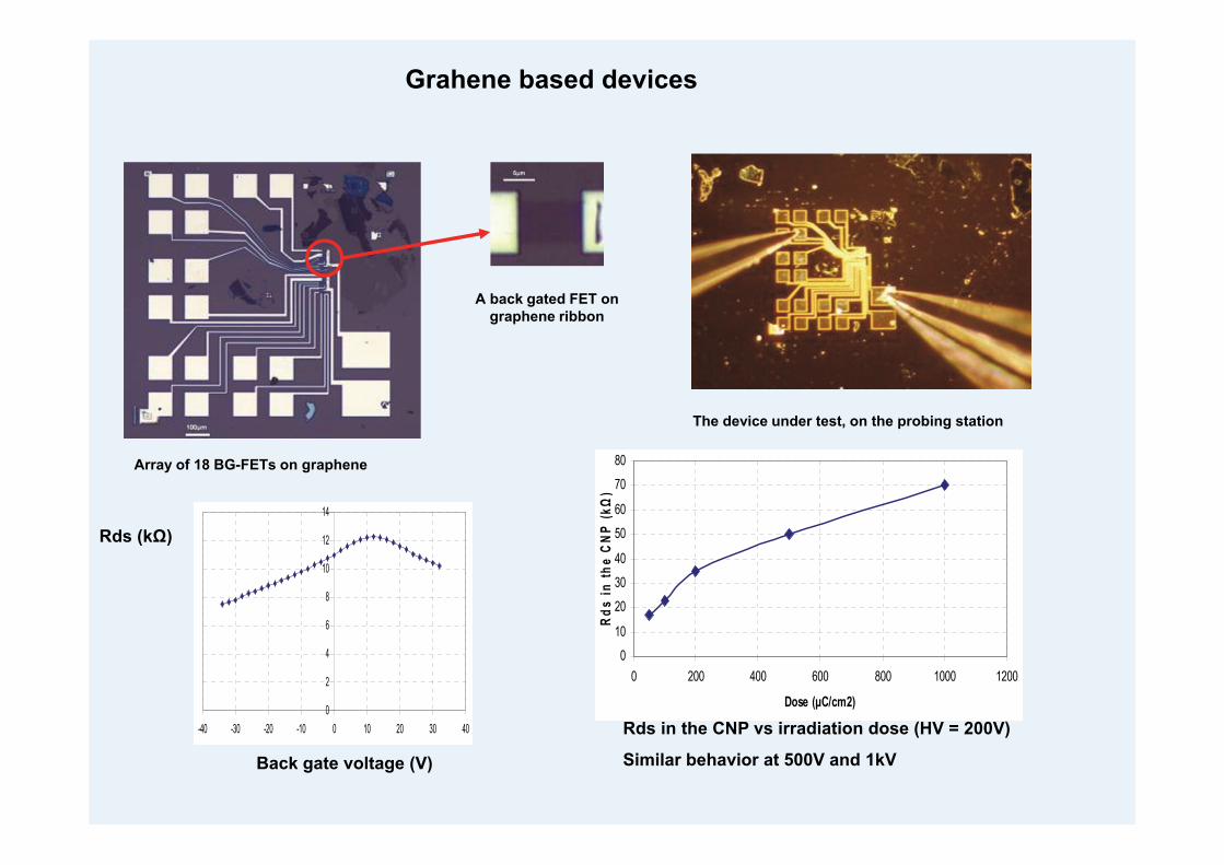
• Technologies for graphene and hybrid MEMS/NEMSo Technologies for graphene synthesis and processingo Development and processing of graphene based hybrid materials for structural health
monitoring microsystemso Technologies for graphene nanoribbons functionalization and integration in
MEMS/NEMS• Technologies for nanocrystalline diamond and applications in MEMS/NEMS and precision
mechanicso Technologies for growth and processing of nanocrystalline diamond structureso Advanced technologies for nanocrystalline diamond-based sensors applied in
scanning probe microscopyo Processing of micro- and nanostructures for nanocrystalline diamond resonators
Research Directions
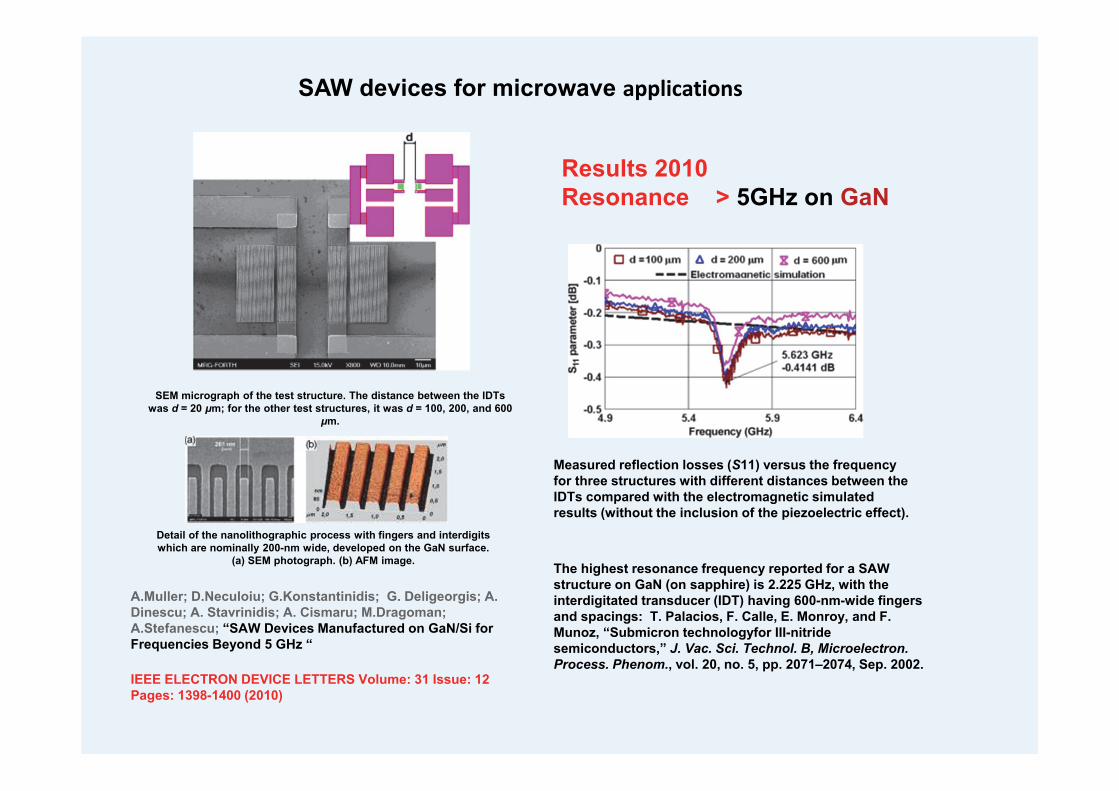
The highest resonance frequency reported for a SAW structure on GaN (on sapphire) is 2.225 GHz, with the interdigitated transducer (IDT) having 600-nm-wide fingers and spacings: T. Palacios, F. Calle, E. Monroy, and F. Munoz, “Submicron technologyfor III-nitride semiconductors,” J. Vac. Sci. Technol. B, Microelectron. Process. Phenom., vol. 20, no. 5, pp. 2071–2074, Sep. 2002.
A.Muller; D.Neculoiu; G.Konstantinidis; G. Deligeorgis; A. Dinescu; A. Stavrinidis; A. Cismaru; M.Dragoman; A.Stefanescu; “SAW Devices Manufactured on GaN/Si for Frequencies Beyond 5 GHz “
SEM micrograph of the test structure. The distance between the IDTs was d = 20 μm; for the other test structures, it was d = 100, 200, and 600
μm.
Measured reflection losses (S11) versus the frequency for three structures with different distances between the IDTs compared with the electromagnetic simulated results (without the inclusion of the piezoelectric effect).
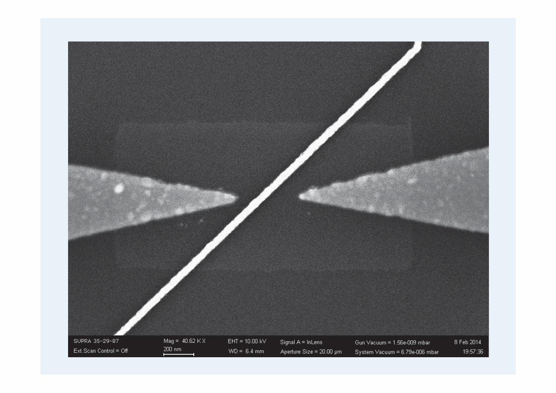
Detail of the nanolithographic process with fingers and interdigits which are nominally 200-nm wide, developed on the GaN surface.