170
Protocoale de Comunicație - curs - Șl. dr. ing. Lucian – Florentin BĂRBULESCU - Craiova, 2019-
Protocoale de Comunicație
- curs -
Șl. dr. ing. Lucian – Florentin BĂRBULESCU
- Craiova, 2019-

Arhitectura Sistemelor Distribuite
2
Cuprins
Cuprins ................................................................................................................. 2
1. Arhitectura Sistemelor Distribuite ................................................................ 5
1.1. Introducere .................................................................................................................... 5
1.2. Clasificarea rețelelor de comunicație .......................................................................... 5
1.3. Evoluția istorică ............................................................................................................ 6
1.3.1. Rețele de calculatoare personale ............................................................................... 8
1.3.2. Rețele de comunicație în domeniul public ............................................................... 8
1.3.3. Rețele locale ............................................................................................................. 9
1.4. Standarde în domeniul comunicației de date ........................................................... 11
2. The physical layer.......................................................................................... 16
2.1. Conducted Media ........................................................................................................ 16
2.1.1. Twisted pair wire .................................................................................................... 16
2.1.2. Coaxial Cable ......................................................................................................... 22
2.1.3. Fiber-optic cable ..................................................................................................... 24
2.2. Wireless Media ............................................................................................................ 26
2.2.1. Terrestrial Microwave Transmission ...................................................................... 27
2.2.2. Satellite Microwave Transmission ......................................................................... 28
2.2.3. Bluetooth ................................................................................................................ 31
2.2.4. Wireless Local Area Networks ............................................................................... 31
3. Data and Signals ............................................................................................ 33
3.1. Introduction ................................................................................................................. 33
3.2. Fundamentals of signals ............................................................................................. 37
3.3. Converting Data into Signals ..................................................................................... 40
3.3.1. Transmitting analog data with analog signals ........................................................ 42
3.3.2. Transmitting digital data with digital signals ......................................................... 43
3.3.3. Transmitting digital data with discrete analog signals ........................................... 48
3.3.4. Transmitting analog data with digital signals ......................................................... 53
3.4. Signal Propagation Delay ........................................................................................... 57
Arhitectura Sistemelor Distribuite
3
3.5. Sources of signal impairments ................................................................................... 59
3.5.1. Attenuation ............................................................................................................. 60
3.5.2. Delay distortion ...................................................................................................... 62
3.5.3. Noise ....................................................................................................................... 62
3.5.4. Limited bandwidth .................................................................................................. 66
3.6. Channel capacity ......................................................................................................... 66
3.6.1. Nyquist Bandwidth ................................................................................................. 67
3.6.2. Shannon Capacity Formula .................................................................................... 68
3.6.3. The expression Eb / N0 ............................................................................................ 69
4. Data Transmission......................................................................................... 71
4.1. Data codes .................................................................................................................... 71
4.1.1. ASCII ...................................................................................................................... 71
4.1.2. Unicode ................................................................................................................... 73
4.2. Transmission modes ................................................................................................... 73
4.2.1. Asynchronous transmission .................................................................................... 74
4.2.2. Synchronous transmission ...................................................................................... 80
5. Data Link Control Protocols ........................................................................ 90
5.1. Error Detection ........................................................................................................... 91
5.1.1. Parity ....................................................................................................................... 92
5.1.2. Block sum check ..................................................................................................... 93
5.1.3. Arithmetic checksum .............................................................................................. 95
5.1.4. Cyclic redundancy check ........................................................................................ 96
5.2. Forward Error Control ............................................................................................ 101
5.3. Feedback Error Control ........................................................................................... 104
5.3.1. Idle RQ ................................................................................................................. 104
5.3.2. Continuous RQ ..................................................................................................... 106
5.4. Flow control ............................................................................................................... 112
5.4.1. Sequence numbers ................................................................................................ 113
5.4.2. Performance Issues ............................................................................................... 115
6. Serial Communication Standards .............................................................. 122
6.1. Electrical Interfaces .................................................................................................. 122
6.1.1. RS-232C/V.24 ...................................................................................................... 122
6.1.2. RS-422/V.11 ......................................................................................................... 125
6.2. Connectors ................................................................................................................. 126
6.3. Physical layer interface standards ........................................................................... 128
6.3.1. RS-232C/V.24 ...................................................................................................... 128
6.3.2. RS-449/V.35 ......................................................................................................... 134
6.4. Transmission control circuits .................................................................................. 134
Arhitectura Sistemelor Distribuite
4
6.4.1. Asynchronous transmission .................................................................................. 135
6.4.2. Synchronous transmission .................................................................................... 139
7. Universal Serial Bus .................................................................................... 142
7.1. History ........................................................................................................................ 142
7.2. Architectural Overview ............................................................................................ 143
7.2.1. Bus components .................................................................................................... 143
7.2.2. Topology ............................................................................................................... 143
7.2.3. Bus speed considerations ...................................................................................... 144
7.2.4. Terminology ......................................................................................................... 146
7.3. Division of labor ........................................................................................................ 147
7.3.1. Host responsibilities ............................................................................................. 147
7.3.2. Device responsibilities .......................................................................................... 150
7.4. Connectors ................................................................................................................. 152
7.4.1. Standard connectors .............................................................................................. 153
7.4.2. Mini and micro connectors ................................................................................... 154
7.4.3. USB 3.0 Connectors ............................................................................................. 154
7.5. Cables ......................................................................................................................... 157
7.5.1. Low-Speed Cables ................................................................................................ 157
7.5.2. Full- and High-Speed Cables ................................................................................ 158
7.5.3. SuperSpeed cable .................................................................................................. 158
7.6. Inside USB Transfers ................................................................................................ 159
7.6.1. Managing data on the bus ..................................................................................... 161
7.6.2. Elements of a transfer ........................................................................................... 161
7.6.3. Transaction types .................................................................................................. 163
7.6.4. USB 2.0 transfers .................................................................................................. 163
7.6.5. SuperSpeed transfers ............................................................................................ 168
Arhitectura Sistemelor Distribuite
5
1. Arhitectura Sistemelor Distribuite
1.1. Introducere
Sistemele de calcul distribuit realizează prelucrarea informației precum și comunicarea
între grupuri distribuite de echipamente de calcul. În general, diferitele tipuri de echipamente
de calcul vor fi numite în continuare DTE (Data Terminal Equipment). Acestea nu includ
numai grupuri distribuite de calculatoare, dar și o gamă variată de echipamente cum ar fi:
terminale video inteligente, stații de lucru, echipamente inteligente pentru controlul proceselor
industriale etc. Varietatea acestor echipamente implică existenta mai multor tipuri de sisteme
distribuite.
Înainte de a se trece la proiectarea elementelor unui sistem de comunicații de date ce va
fi folosit într-un sistem distribuit dat, trebuie cunoscute două lucruri:
diferitele tipuri de rețele de comunicație disponibile, modurile acestora de lucru
(operare), domeniile de operabilitate;
setul de standarde internaționale ce a fost elaborat în vederea ușurării folosirii acestor
rețele.
1.2. Clasificarea rețelelor de comunicație
Rețelele de comunicație pot fi clasificate în patru categorii în funcție de distanța fizică
dintre elementele ce comunică între ele:
1. Rețele miniaturale (< 5cm). Acestea realizează interconectarea diferitelor elemente de
calcul ce sunt implementate pe același circuit integrat.
2. Rețele mici (< 50 cm). Acestea realizează interconectarea unităților de calcul localizate
în aceeași cutie sau subansamblu al unui echipament.
Arhitectura Sistemelor Distribuite
6
3. Rețele medii (< 10 km). Realizează interconectarea echipamentelor de calcul (stații de
lucru, aparate de măsură inteligente) distribuite pe o arie limitată. Aceste rețele se mai
numesc și rețele locale (LAN – Local Area Networks).
4. Rețele mari (>10 km). Realizează interconectarea diferitelor module ale unui sistem de
calcul cum ar fi: mainframe sau minicalculatoare, terminale inteligente etc. Acestea
sunt distribuite pe o suprafață mai întinsă (suprafața unei țări sau arii geografice mai
întinse). Rețelele de acest tip se mai numesc și rețele globale (WAN – Wide Area
Networks).
În cazul primelor două tipuri de rețele, datorită distanței mici dintre elementele de
calcul, toate mesajele sunt transferate în mod paralel. Aceste rețele fac parte din categoria
rețelelor puternic conectate (CCS – Closely Coupled Systems).
Celelalte două tipuri de rețele fac parte din categoria sistemelor slab conectate (LCS –
Loosely Coupled Systems), transferul mesajelor făcându-se în mod serial.
În general, prima categorie de rețele (CCS) realizează schimbul de date între elemente
de calcul omogene. În contrast, sistemele slab conectate (LCS) realizează schimbul de date
între calculatoare sau echipamente de tipuri diferite. Principalele obiective ale acestor sisteme
sunt:
să asigure transferuri de date fără erori;
să asigure ca mesajele transferate să aibă aceeași semnificație în toate sistemele.
Pentru a realiza aceste obiective LCS folosesc diferite forme de rețele și protocoale de
comunicație. Acesta este tipul de sisteme ce face obiectul cursului.
1.3. Evoluția istorică
Evoluția LCS a fost determinată de dezvoltarea resurselor folosite în cadrul unui sistem
de calcul.
Primele calculatoare comerciale au fost caracterizate printr-un harware voluminos și
software primitiv. Cu timpul, datorită progresului tehnologic și dezvoltării software-ului au
apărut unitățile de discuri magnetice și sistemele de operare de tip multiuser. Aceasta a făcut
posibilă partajarea în timp a CPU între mai multe programe active, permițând mai multor
utilizatori să-și execute programele interactiv și să aibă acces simultan la datele memorate
prin intermediul unui terminal separat.
Arhitectura Sistemelor Distribuite
7
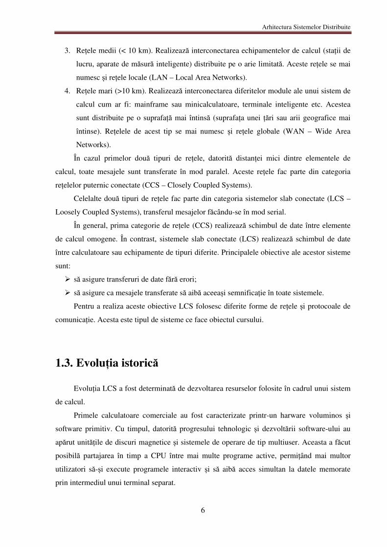
Pentru a valorifica aceste realizări calculatoarele au fost proiectate astfel încât să suporte
mai multe terminale. Astfel de calculatoare au fost numite sisteme multi-acces permițând
accesul on-line la datele memorate. Prin intermediul modem-urilor și rețelelor telefonice,
terminalele au putut fi plasate la distanțe mari de calculator (figura 1.1 a).
Folosirea rețelelor telefonice ca mediu principal pentru comunicația de date a făcut ca în
curând costul unei linii de comunicație să nu mai fie nesemnificativ. De aceea au fost
introduse multiplexoare statistice și dispozitive de tip “cluster controller” astfel încât o
singură linie de comunicație să fie folosită de mai mulți utilizatori aflați în același loc (figura
1.1 b).
Arhitectura Sistemelor Distribuite
8
În plus, creșterea foarte mare a numărului de terminale (la câteva sute) a impus
introducerea FEP (Front-End Processor) care degrevează CPU de sarcina comunicării.
1.3.1. Rețele de calculatoare personale
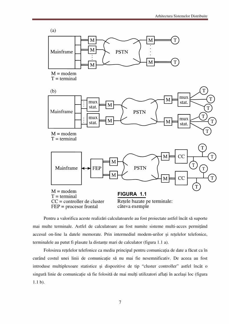
Structurile prezentate în figurile anterioare se caracterizează prin concentrarea unei mari
cantități de informații într-un singur loc. În astfel de structuri, utilizatorii dispersați în spațiu,
accesează și actualizează informația folosind diverse facilități de comunicare (figura 1.2).
În multe cazuri însă, nu este nevoie ca informația să fie stocată centralizat. De aceea se
preferă plasarea în diverse locuri a unor sisteme de calcul autonome. Aceste sisteme pot
funcționa independent, dar de multe ori este nevoie să schimbe informații sau să-și partajeze
resurse hardware sau software.
Pentru o astfel de rețea a apărut limitarea volumului de date schimbate datorată rețelei
telefonice și modem-urilor. Astfel a apărut necesitatea realizării unor rețele de comunicație
independente. Cerințele impuse unor astfel de rețele au fost în mare măsură similare
caracteristicilor rețelelor de telex.
1.3.2. Rețele de comunicație în domeniul public
Arhitectura Sistemelor Distribuite
9
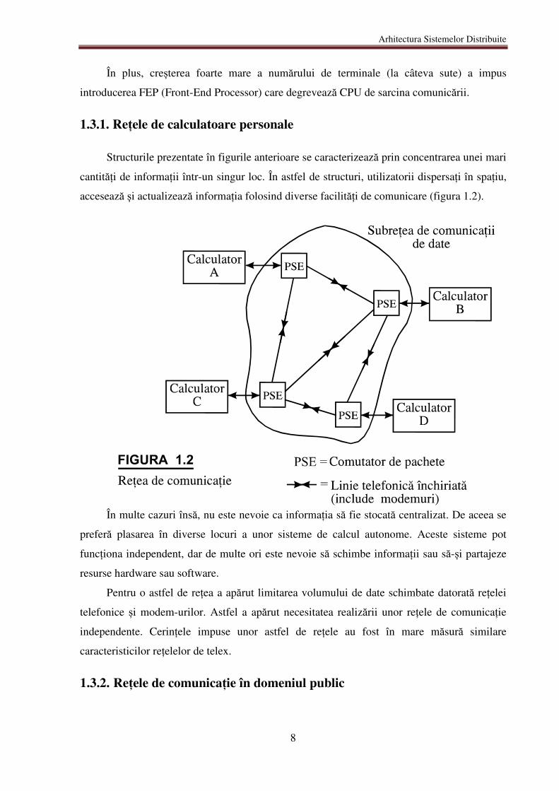
Inițial, rețelele de comunicație au fost realizate la nivel național, folosind linii de
telecomunicație închiriate. Cu timpul, a apărut necesitatea comunicării între două calculatoare
aparținând la două rețele diferite. În acest moment multe țări au acceptat faptul că analog
rețelei telefonice (PSTN – Public Switched Telephone Network) trebuie să existe o rețea de
comunicații de date (PSDN - Public Switched Data Network). În plus, datorită faptului că
această rețea trebuia să permită comunicarea între diferite tipuri de echipamente a devenit
necesară adoptarea unor standarde de interfațare.
După multe discuții, mai întâi la nivel național și apoi la nivel internațional, a fost
adoptat un set de standarde internaționale cu rolul de a interfața și controla fluxul de
informații între un DTE și diferite tipuri de PSDN (figura 1.3).
1.3.3. Rețele locale
Datorită evoluției tehnologice și implicit a dezvoltării resurselor de calcul numărul
echipamentelor de calcul a crescut foarte mult. Astfel au devenit comune structuri alcătuite
din mai multe stații de lucru (executând de exemplu procesare de texte) localizate fizic în
aceeași clădire. Fiecare din aceste stații poate executa independent numeroase sarcini, dar de
multe ori este necesară și comunicarea între ele (în scopul transferului de fișiere sau pentru
Arhitectura Sistemelor Distribuite
10
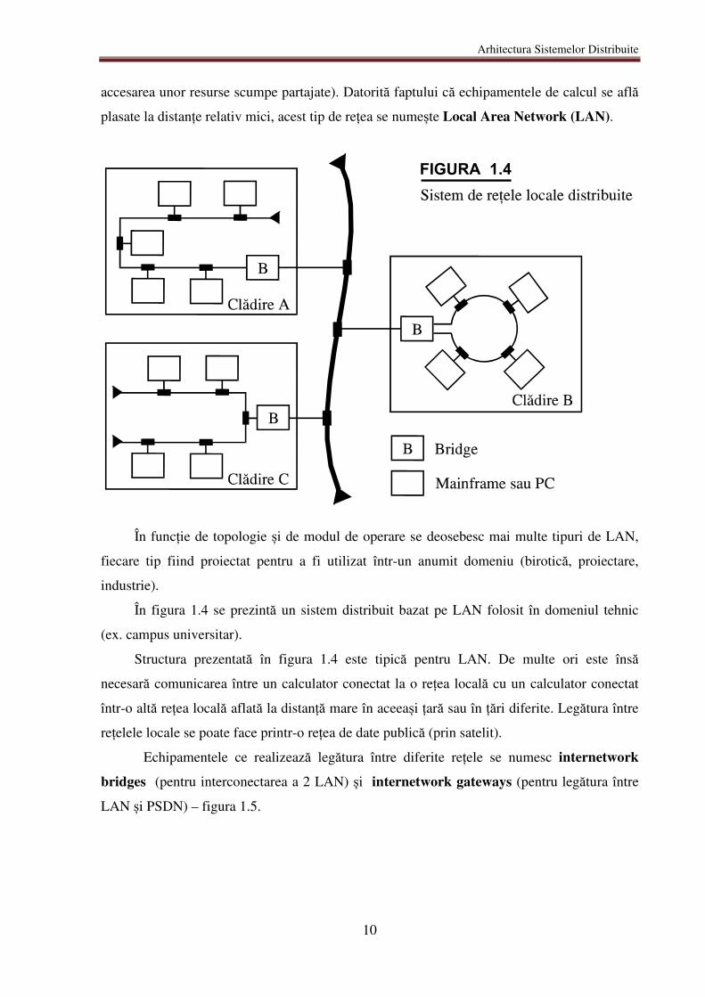
accesarea unor resurse scumpe partajate). Datorită faptului că echipamentele de calcul se află
plasate la distanțe relativ mici, acest tip de rețea se numește Local Area Network (LAN).
În funcție de topologie și de modul de operare se deosebesc mai multe tipuri de LAN,
fiecare tip fiind proiectat pentru a fi utilizat într-un anumit domeniu (birotică, proiectare,
industrie).
În figura 1.4 se prezintă un sistem distribuit bazat pe LAN folosit în domeniul tehnic
(ex. campus universitar).
Structura prezentată în figura 1.4 este tipică pentru LAN. De multe ori este însă
necesară comunicarea între un calculator conectat la o rețea locală cu un calculator conectat
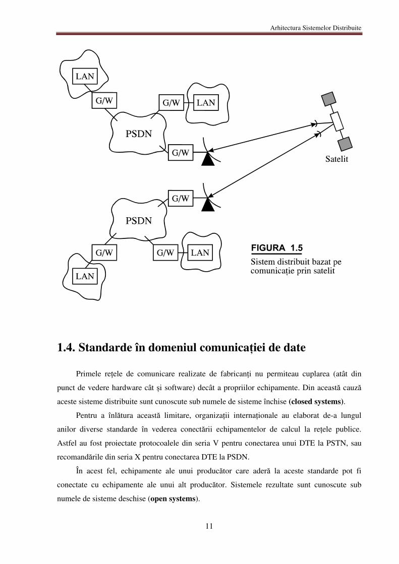
într-o altă rețea locală aflată la distanță mare în aceeași țară sau în țări diferite. Legătura între
rețelele locale se poate face printr-o rețea de date publică (prin satelit).
Echipamentele ce realizează legătura între diferite rețele se numesc internetwork
bridges (pentru interconectarea a 2 LAN) și internetwork gateways (pentru legătura între
LAN și PSDN) – figura 1.5.
Arhitectura Sistemelor Distribuite
11
1.4. Standarde în domeniul comunicației de date
Primele rețele de comunicare realizate de fabricanți nu permiteau cuplarea (atât din
punct de vedere hardware cât și software) decât a propriilor echipamente. Din această cauză
aceste sisteme distribuite sunt cunoscute sub numele de sisteme închise (closed systems).
Pentru a înlătura această limitare, organizații internaționale au elaborat de-a lungul
anilor diverse standarde în vederea conectării echipamentelor de calcul la rețele publice.
Astfel au fost proiectate protocoalele din seria V pentru conectarea unui DTE la PSTN, sau
recomandările din seria X pentru conectarea DTE la PSDN.
În acest fel, echipamente ale unui producător care aderă la aceste standarde pot fi
conectate cu echipamente ale unui alt producător. Sistemele rezultate sunt cunoscute sub
numele de sisteme deschise (open systems).
Arhitectura Sistemelor Distribuite
12
Începând din anul 1970 au început să se înmulțească tipurile de sisteme distribuite. De
aceea au fost introduse tot mai multe standarde de comunicație. Primul standard introdus
privea structura generală a unui sistem de comunicare între calculatoare. Acesta a fost
proiectat de International Standards Organization (ISO) și a fost cunoscut sub numele de ISO
Reference Model for Open Systems Interconnection (OSI).
Scopul ISO Reference Model for OSI a fost de a stabili o bază comună pentru
coordonarea dezvoltării standardelor în domeniul interconectării sistemelor.
Termenul "Open Systems Interconnection" desemnează standarde privind schimbul de
informație între sisteme deschise. Faptul că un sistem este deschis nu presupune o
implementare, tehnologie sau interconectare particulară ci se referă la recunoașterea sau
aplicarea mutuală a standardelor.
Un alt obiectiv al ISO este de a identifica domeniile în care standardele pot fi dezvoltate
sau îmbunătățite și de a menține consistența standardelor înrudite.
Tehnica de structurare adoptată de ISO este cea a stratificării. Funcțiile de comunicație
sunt separate pe mai multe nivele (layers). Fiecare nivel realizează un subset de funcții
necesare pentru comunicația cu un alt sistem. Ideal este ca nivelele să fie astfel definite încât
modificări efectuate într-un nivel să nu necesite modificări și în alte nivele.
Sarcina ISO a fost să definească un set de nivele și serviciile realizate de fiecare nivel.
Principiile avute în vedere de ISO au fost următoarele:
5. Să nu se creeze mai multe nivele decât sunt necesare deoarece devine mai dificilă
descrierea și integrarea nivelelor.
6. Crearea unei granițe la un punct unde descrierea serviciilor poate fi mică și numărul
interacțiunilor între nivele este minim.
7. Crearea de nivele separate pentru funcții ce se manifestă diferit în timpul derulării
procesului.
8. Gruparea funcțiilor similare în același nivel.
9. Selectarea granițelor în puncte alese pe baza experienței anterioare.
10. Crearea unui nivel pe baza unor funcții ce pot fi ușor localizate astfel încât
reproiectarea sa totală sau modificarea protocoalelor datorită progresului tehnologic
hardware sau software să nu necesite modificarea serviciilor așteptate de la sau
furnizate pentru nivelele adiacente.
11. Crearea unei granițe în punctul în care la un moment dat s-ar putea să avem o interfață
corespunzătoare standardizată.
Arhitectura Sistemelor Distribuite
13
12. Crearea unui nivel atunci când se trece la un nivel diferit de abstractizare a datelor (ex.
morfologie, sintaxa, semantică).
13. Să permită schimbarea funcțiilor și protocoalelor dintr-un nivel fără a afecta celelalte
nivele.
14. Fiecare nivel să se învecineze numai cu nivelul superior și cu cel inferior lui.
Avantajul modelului OSI îl reprezintă rezolvarea comunicației între calculatoare
eterogene. Două sisteme, indiferent cât se deosebesc, pot comunica efectiv dacă îndeplinesc
următoarele condiții:
Implementează același set de funcții de comunicație.
Aceste funcții sunt organizate în cadrul aceluiași set de nivele. Nivelele pereche trebuie
să realizeze aceleași funcții, dar nu este necesar să le realizeze în același mod.
Nivelele pereche trebuie să folosească un protocol comun.
Plecând de la principiile enunțate, modelul OSI a definit un set de șapte nivele.
Nivelul fizic (physical layer) acoperă interfața fizică între echipamente și regulile prin
care biții sunt transferați de la unul la altul. Acesta oferă numai un serviciu de transfer al
șirurilor de biți. Nivelul fizic are patru caracteristici importante:
mecanice
electrice
funcționale
procedurale
Nivelul legăturii de date (data link layer) are rolul de a face sigură legătura fizică
precum și de a activa, întreține și dezactiva legătura. Principalul serviciu pe care acest nivel îl
oferă nivelului superior este controlul erorilor.
Nivelul rețea (network layer) are rolul de a realiza transferul transparent al datelor
între entitățile de transport. El permite nivelului superior (transport) să știe totul despre
transmisia de date din nivelele inferioare și să aleagă tehnologia folosită pentru conectarea
sistemelor.
Nivelul transport (transport layer) realizează un mecanism sigur de schimb de date
între procese din sisteme diferite. Acest nivel asigură transmiterea fără erori și în secvență
corectă a unităților de date.
Nivelul sesiune (session layer) propune un mecanism pentru controlarea dialogului
între aplicații.
Nivelul prezentare (presentation layer) se ocupă cu sintaxa schimbului de date între
aplicații. Își propune să rezolve diferențele dintre formatele de reprezentare a datelor.
Arhitectura Sistemelor Distribuite
14
Nivelul aplicație (application layer) creează un mijloc prin care aplicațiile să acceseze
mediul OSI. Acest nivel conține funcții de gestionare și mecanisme general valabile pentru
aplicații distribuite.
În figura 1.6 este ilustrat modelul OSI:
Fiecare sistem conține câte șapte nivele. Comunicația se realizează între aplicațiile
notate AP X și AP Y din cele două sisteme. Dacă AP X dorește să transmită un mesaj către
AP Y atunci este solicitat nivelul 7. Acesta stabilește o relație de tip "peer-to-peer" cu nivelul
7 al sistemului receptor, folosind un protocol specific acestui nivel. Acest protocol folosește
servicii oferite de nivelul 6. La rândul său, nivelul 6 folosește un protocol propriu și așa mai
departe până la nivelul fizic care realizează transmisia biților prin mediul de transmisie.
Observație: Între nivelele pereche nu există o comunicație directă cu excepția nivelului
fizic.
Atunci când aplicația X are de transmis un mesaj către aplicația Y, informația este
transferată către "application layer". Aici se adaugă un antet (header) ce conține informație
necesară protocolului corespunzător nivelului 7 pereche (operația se numește încapsulare).
Datele originale plus acest antet sunt transferate sub forma unei unități de date către nivelul 6.

Arhitectura Sistemelor Distribuite
15
"Presentation layer" tratează întreaga entitate ca pe o dată și Ti adaugă propriul antet (a doua
încapsulare). Acest proces continuă în jos până la nivelul 2 care, în general, adaugă datelor
atât un antet cât și o coadă. Entitatea rezultată poartă numele de pachet și este transferată prin
nivelul fizic către mediul de transmisie. Când pachetul este recepționat de sistemul destinație
are loc un proces invers. Fiecare nivel își extrage antetul corespunzător conținând informații
solicitate de protocolul folosit în comun la acel nivel.
The physical layer
16
2. The physical layer
The data communication would not exist if there were no medium by which to transfer
data. All communications media can be divided into two categories: (1) physical or conducted
media, such as telephone lines, computer networks and fiber-optic cables, and (2) radiated or
wireless media, such as cell phones, wireless networks and satellite systems.
Conducted media include twisted pair wire, coaxial cable, and fiber-optic cable while
from the wireless media one can mention terrestrial microwave, satellite transmissions,
Bluetooth and wireless local area network systems.
2.1. Conducted Media
Even though conducted media have been around as long as the telephone itself (even
longer if you include the telegraph), there have been few recent or unique additions to this
technology. The newest member of the conducted media family—fiber-optic cable—became
widely used by telephone companies in the 1980s and by computer network designers in the
1990s. But let us begin our discussion of the three existing types of conducted media with the
oldest, simplest, and most common one: twisted pair wire.
2.1.1. Twisted pair wire
The term “twisted pair” is almost a misnomer, as one rarely encounters a single pair of
wires. More often, twisted pair wire comes as two or more pairs of single-conductor copper
wires that have been twisted around each other. Each single-conductor wire is encased within
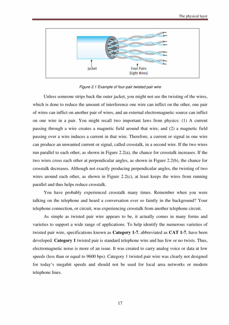
plastic insulation and cabled within one outer jacket, as shown in Figure 2.1.
The physical layer
17
Figure 2.1 Example of four-pair twisted pair wire
Unless someone strips back the outer jacket, you might not see the twisting of the wires,
which is done to reduce the amount of interference one wire can inflict on the other, one pair
of wires can inflict on another pair of wires, and an external electromagnetic source can inflict
on one wire in a pair. You might recall two important laws from physics: (1) A current
passing through a wire creates a magnetic field around that wire, and (2) a magnetic field
passing over a wire induces a current in that wire. Therefore, a current or signal in one wire
can produce an unwanted current or signal, called crosstalk, in a second wire. If the two wires
run parallel to each other, as shown in Figure 2.2(a), the chance for crosstalk increases. If the
two wires cross each other at perpendicular angles, as shown in Figure 2.2(b), the chance for
crosstalk decreases. Although not exactly producing perpendicular angles, the twisting of two
wires around each other, as shown in Figure 2.2(c), at least keeps the wires from running
parallel and thus helps reduce crosstalk.
You have probably experienced crosstalk many times. Remember when you were
talking on the telephone and heard a conversation ever so faintly in the background? Your
telephone connection, or circuit, was experiencing crosstalk from another telephone circuit.
As simple as twisted pair wire appears to be, it actually comes in many forms and
varieties to support a wide range of applications. To help identify the numerous varieties of
twisted pair wire, specifications known as Category 1-7, abbreviated as CAT 1-7, have been
developed. Category 1 twisted pair is standard telephone wire and has few or no twists. Thus,
electromagnetic noise is more of an issue. It was created to carry analog voice or data at low
speeds (less than or equal to 9600 bps). Category 1 twisted pair wire was clearly not designed
for today’s megabit speeds and should not be used for local area networks or modern
telephone lines.

The physical layer
18
Figure 2.2 (a) Parallel wires— greater chance of crosstalk (b) Perpendicular wires—less chance of crosstalk (c) Twisted wires—crosstalk reduced because wires keep crossing each other at nearly
perpendicular angles
Category 2 twisted pair wire was also used for telephone circuits and some low-speed
LANs but has some twisting, thus producing less noise. Category 2 twisted pair is sometimes
found on T-1 and ISDN lines and in some installations of standard telephone circuits. T-1 is
the designation for a digital telephone circuit that transmits voice or data at 1.544 Mbps.
ISDN is a digital telephone circuit that can transmit voice or data or both from 64 kbps to
1.544 Mbps. Once again, advances in twisted pair wire such as the use of more twists are
leading to Category 2 wire being replaced with higher-quality wire, so it is very difficult to
locate anyone still selling this wire. But even if they were selling it, you would never use it for
a modern network.
Category 3 twisted pair was designed to transmit 10 Mbps of data over a local area
network for distances up to 100 meters. Although the signal does not magically stop at 100
meters, it does weaken (attenuate), and the level of noise continues to grow such that the
likelihood of the wire transmitting errors after 100 meters increases. The constraint of no
more than 100 meters applies to the distance from the device that generates the signal (the
source) to the device that accepts the signal (the destination). This accepting device can be
either the final destination or a repeater. A repeater is a device that generates a new signal by
creating an exact replica of the original signal. Thus, Category 3 twisted pair can run farther
than 100 meters from its source to its final destination, as long as the signal is regenerated at

The physical layer
19
least every 100 meters. Much of the Category 3 wire sold today is used for simple telephone
circuits instead of computer network installations.
Category 4 twisted pair was designed to transmit 20 Mbps of data for distances up to
100 meters. It was created at a time when local area networks required a wire that could
transmit data faster than the 10-Mbps speed of Category 3. Category 4 wire is rarely, if ever,
sold anymore, and essentially has been replaced with newer types of twisted pair.
Category 5 twisted pair was designed to transmit 100 Mbps of data for distances up to
100 meters. (Technically speaking, Category 5 is specified for a 100-MHz signal, but because
most systems transmit 100 Mbps over the 100-MHz signal, 100 MHz is equivalent to 100
Mbps.) Category 5 twisted pair has a higher number of twists per inch than the Category 1 to
4 wires and, thus, introduces less noise.
Approved at the end of 1999, the specification for Category 5e twisted pair is similar to
Category 5’s in that this wire is also recommended for transmissions of 100 Mbps (100 MHz)
for 100 meters. Many companies are producing Category 5e wire at 125 MHz for 100 meters.
Although the specifications for the earlier Category 1 to 5 wires describe only the individual
wires, the Category 5e specification indicates exactly four pairs of wires and provides
designations for the connectors on the ends of the wires, patch cords, and other possible
components that connect directly with a cable. Thus, as a more detailed specification than
Category 5, Category 5e can better support the higher speeds of 100-Mbps (and higher) local
area networks. It is the minimum twisted-pair cable that supports 1000-Mps (or gigabit)
networks by using all four pairs in the same time and also by encoding more than one bit in a
signal. More about encoding in the following sub-chapter.
Category 6 twisted pair is designed to support data transmission with signals as high as
250 MHz for 100 meters. It has a plastic spacer running down the middle of the cable that
separates the twisted pairs and further reduces electromagnetic noise. This makes Category 6
wire a good choice for 100-meter runs in local area networks with transmission speeds of 250
to 1000 Mbps.
Interestingly, Category 6 twisted pair costs only a little more than Category 5e twisted
pair wires. Therefore, given a choice of Category 5, 5e, or 6 twisted pair wires, you probably
should install Category 6—in other words, the best-quality wire—regardless of whether or not
you will be taking immediate advantage of the higher transmission speeds.
Category 7 twisted pair is the most recent addition to the twisted pair family. Category
7 wire is designed to support 600 MHz of bandwidth for 100 meters. The cable is heavily

The physical layer
20
shielded—each pair of wires is shielded by a foil, and the entire cable has a shield as well. It
can be used for very high speed networks like the 10-Gigabit Ethernet.
All of the wires described so far with the exception of Category 7 wire can be purchased
as unshielded twisted pair. Unshielded twisted pair (UTP) is the most common form of
twisted pair; none of the wires in this form is wrapped with a metal foil or braid. In contrast,
shielded twisted pair (STP), which also is available in Category 5 to 6 (as well as numerous
wire configurations), is a form in which a shield is wrapped around each wire individually,
around all the wires together, or both. This shielding provides an extra layer of isolation from
unwanted electromagnetic interference. Figure 2.3 shows an example of shielded twisted pair
wire.
Figure 2.3 An example of shielded twisted pair wire
If a twisted pair wire needs to go through walls, rooms, or buildings where there is
sufficient electromagnetic interference to cause substantial noise problems, using shielded
twisted pair can provide a higher level of isolation from that interference than unshielded
twisted pair wire and, thus, a lower level of errors. (You can also run the twisted pair wire
through a metal conduit.) Electromagnetic interference is often generated by large motors,
such as those found in heating and cooling equipment or manufacturing equipment. Even
fluorescent light fixtures generate a noticeable amount of electromagnetic interference. Large
sources of power can also generate damaging amounts of electromagnetic interference.
Therefore, it is generally not a good idea to strap twisted pair wiring to a power line that runs
through a room or through walls. Furthermore, even though Category 5 to 6 shielded twisted
pair wires have improved noise isolation, you cannot expect to push them past the 100-meter
limit. And, of course, the price per meter of a shielded twisted pair cable is greater than the
price for a unshielded twisted pair cable.
Table 2-1 A summary of the characteristics of twisted pair wires
UTP
Category
Typical Use Maximum
Data
Maximum
Transmission
Advantages Disadvantages

The physical layer
21
Transfer
Rate
Range
Category 1 Telephone wire <100 kbps
5–6 kilometers
Inexpensive, easy to install and interface
Security, noise, obsolete
Category 2 T-1, ISDN <2 Mbps 5–6 kilometers
Same as Category 1
Security, noise, obsolete
Category 3 Telephone circuits 10 Mbps 100 m
Same as Category 1, with less noise Security, noise
Category 4 LANs 20 Mbps 100 m
Same as Category 1, with less noise
Security, noise, obsolete
Category 5 LANs 100 Mbps (100 MHz) 100 m
Same as Category 1, with less noise Security, noise
Category 5e LANs
250 Mbps per pair (125 MHz) 100 m
Same as Category 5. Also includes specifications for connectors, patch cords, and other components Security, noise
Category 6 LANs
250 Mbps per pair (250 MHz) 100 m
Higher rates than Category 5e, less noise
Security, noise, cost
Category 7 LANs 600 MHz 100 m High data rates
Security, noise, cost
Table 2-1 summarizes the basic characteristics of unshielded twisted pair wires. Keep in
mind that for our purposes, shielded twisted pair wires have basically the same data transfer
rates and transmission ranges as unshielded twisted pair wires but perform better in noisy
environments. Note also that the transmission distances and transfer rates appearing in Table
2-1 are not etched in stone. Noisy environments tend to shorten transmission distances and
transfer rates.
The physical layer
22
2.1.2. Coaxial Cable
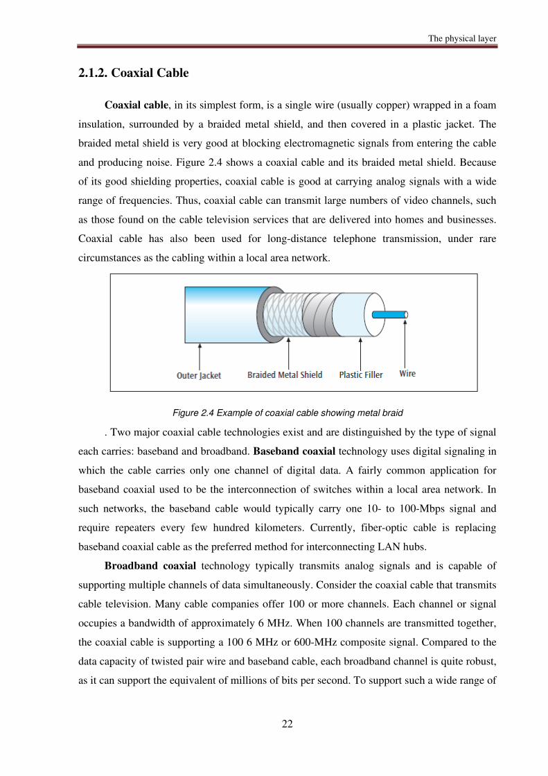
Coaxial cable, in its simplest form, is a single wire (usually copper) wrapped in a foam
insulation, surrounded by a braided metal shield, and then covered in a plastic jacket. The
braided metal shield is very good at blocking electromagnetic signals from entering the cable
and producing noise. Figure 2.4 shows a coaxial cable and its braided metal shield. Because
of its good shielding properties, coaxial cable is good at carrying analog signals with a wide
range of frequencies. Thus, coaxial cable can transmit large numbers of video channels, such
as those found on the cable television services that are delivered into homes and businesses.
Coaxial cable has also been used for long-distance telephone transmission, under rare
circumstances as the cabling within a local area network.
Figure 2.4 Example of coaxial cable showing metal braid
. Two major coaxial cable technologies exist and are distinguished by the type of signal
each carries: baseband and broadband. Baseband coaxial technology uses digital signaling in
which the cable carries only one channel of digital data. A fairly common application for
baseband coaxial used to be the interconnection of switches within a local area network. In
such networks, the baseband cable would typically carry one 10- to 100-Mbps signal and
require repeaters every few hundred kilometers. Currently, fiber-optic cable is replacing
baseband coaxial cable as the preferred method for interconnecting LAN hubs.
Broadband coaxial technology typically transmits analog signals and is capable of
supporting multiple channels of data simultaneously. Consider the coaxial cable that transmits
cable television. Many cable companies offer 100 or more channels. Each channel or signal
occupies a bandwidth of approximately 6 MHz. When 100 channels are transmitted together,
the coaxial cable is supporting a 100 6 MHz or 600-MHz composite signal. Compared to the
data capacity of twisted pair wire and baseband cable, each broadband channel is quite robust,
as it can support the equivalent of millions of bits per second. To support such a wide range of
The physical layer
23
frequencies, broadband coaxial cable systems require amplifiers approximately every three to
four kilometers.
In addition to the two signal-based categories, coaxial cable also is available in a variety
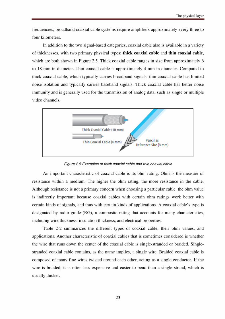
of thicknesses, with two primary physical types: thick coaxial cable and thin coaxial cable,
which are both shown in Figure 2.5. Thick coaxial cable ranges in size from approximately 6
to 18 mm in diameter. Thin coaxial cable is approximately 4 mm in diameter. Compared to
thick coaxial cable, which typically carries broadband signals, thin coaxial cable has limited
noise isolation and typically carries baseband signals. Thick coaxial cable has better noise
immunity and is generally used for the transmission of analog data, such as single or multiple
video channels.
Figure 2.5 Examples of thick coaxial cable and thin coaxial cable
An important characteristic of coaxial cable is its ohm rating. Ohm is the measure of
resistance within a medium. The higher the ohm rating, the more resistance in the cable.
Although resistance is not a primary concern when choosing a particular cable, the ohm value
is indirectly important because coaxial cables with certain ohm ratings work better with
certain kinds of signals, and thus with certain kinds of applications. A coaxial cable’s type is
designated by radio guide (RG), a composite rating that accounts for many characteristics,
including wire thickness, insulation thickness, and electrical properties.
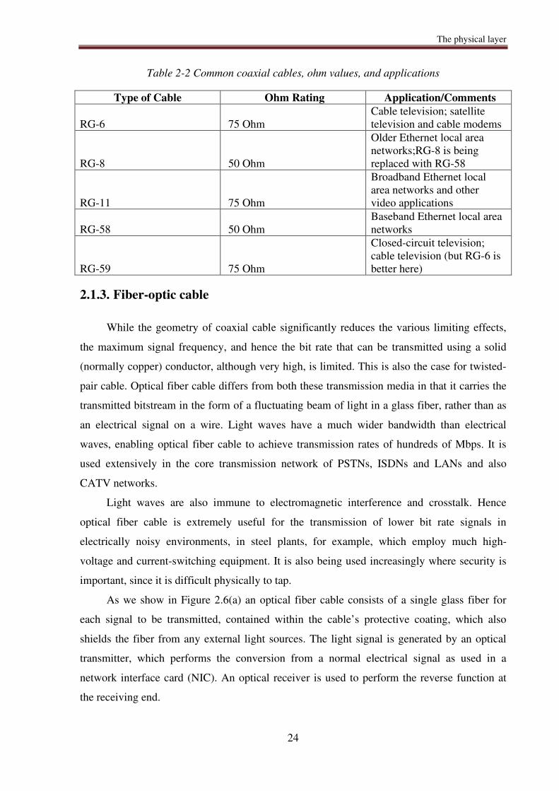
Table 2-2 summarizes the different types of coaxial cable, their ohm values, and
applications. Another characteristic of coaxial cables that is sometimes considered is whether
the wire that runs down the center of the coaxial cable is single-stranded or braided. Single-
stranded coaxial cable contains, as the name implies, a single wire. Braided coaxial cable is
composed of many fine wires twisted around each other, acting as a single conductor. If the
wire is braided, it is often less expensive and easier to bend than a single strand, which is
usually thicker.
The physical layer
24
Table 2-2 Common coaxial cables, ohm values, and applications
Type of Cable Ohm Rating Application/Comments
RG-6 75 Ohm Cable television; satellite television and cable modems
RG-8 50 Ohm
Older Ethernet local area networks;RG-8 is being replaced with RG-58
RG-11 75 Ohm
Broadband Ethernet local area networks and other video applications
RG-58 50 Ohm Baseband Ethernet local area networks
RG-59 75 Ohm
Closed-circuit television; cable television (but RG-6 is better here)
2.1.3. Fiber-optic cable
While the geometry of coaxial cable significantly reduces the various limiting effects,
the maximum signal frequency, and hence the bit rate that can be transmitted using a solid
(normally copper) conductor, although very high, is limited. This is also the case for twisted-
pair cable. Optical fiber cable differs from both these transmission media in that it carries the
transmitted bitstream in the form of a fluctuating beam of light in a glass fiber, rather than as
an electrical signal on a wire. Light waves have a much wider bandwidth than electrical
waves, enabling optical fiber cable to achieve transmission rates of hundreds of Mbps. It is
used extensively in the core transmission network of PSTNs, ISDNs and LANs and also
CATV networks.
Light waves are also immune to electromagnetic interference and crosstalk. Hence
optical fiber cable is extremely useful for the transmission of lower bit rate signals in
electrically noisy environments, in steel plants, for example, which employ much high-
voltage and current-switching equipment. It is also being used increasingly where security is
important, since it is difficult physically to tap.
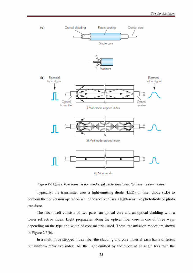
As we show in Figure 2.6(a) an optical fiber cable consists of a single glass fiber for
each signal to be transmitted, contained within the cable’s protective coating, which also
shields the fiber from any external light sources. The light signal is generated by an optical
transmitter, which performs the conversion from a normal electrical signal as used in a
network interface card (NIC). An optical receiver is used to perform the reverse function at
the receiving end.
The physical layer
25
Figure 2.6 Optical fiber transmission media: (a) cable structures; (b) transmission modes.
Typically, the transmitter uses a light-emitting diode (LED) or laser diode (LD) to
perform the conversion operation while the receiver uses a light-sensitive photodiode or photo
transistor.
The fiber itself consists of two parts: an optical core and an optical cladding with a
lower refractive index. Light propagates along the optical fiber core in one of three ways
depending on the type and width of core material used. These transmission modes are shown
in Figure 2.6(b).
In a multimode stepped index fiber the cladding and core material each has a different
but uniform refractive index. All the light emitted by the diode at an angle less than the
The physical layer
26
critical angle is reflected at the cladding interface and propagates along the core by means of
multiple (internal) reflections. Depending on the angle at which it is emitted by the diode, the
light will take a variable amount of time to propagate along the cable. Therefore the received
signal has a wider pulse width than the input signal with a corresponding decrease in the
maximum permissible bit rate. This effect is known as dispersion and means this type of cable
is used primarily for modest bit rates with relatively inexpensive LEDs compared to laser
diodes.
Dispersion can be reduced by using a core material that has a variable (rather than
constant) refractive index. As we show in Figure 2.6(b), in a multi-mode graded index fiber
light is refracted by an increasing amount as it moves away from the core. This has the effect
of narrowing the pulse width of the received signal compared with stepped index fiber,
allowing a corresponding increase in maximum bit rate.
Further improvements can be obtained by reducing the core diameter to that of a single
wavelength (3–10 μm) so that all the emitted light propagates along a single (dispersionless)
path. Consequently, the received signal is of a comparable width to the input signal and is
called monomode fiber. It is normally used with LDs and can operate at hundreds of Mbps.
Alternatively, multiple high bit rate transmission channels can be derived from the same
fiber by using different portions of the optical bandwidth for each channel. This mode of
operation is known as wave-division multiplexing (WDM) and, when using this, bit rates in
excess of tens of Gbps can be achieved.
2.2. Wireless Media
Wireless transmission became popular in the 1950s with AM radio, FM radio, and
television. In 1962, transmissions were sent through the first orbiting satellite, Telstar. In the
60 or so years since wireless transmission emerged, this technology has spawned hundreds, if
not thousands, of applications, some of which will be discussed in this chapter.
In wireless transmission, various types of electromagnetic waves are used to transmit
signals. Radio transmissions, satellite transmissions, visible light, infrared light, X-rays, and
gamma rays are all examples of electromagnetic waves or electromagnetic radiation. In
general, electromagnetic radiation is energy propagated through space and, indirectly, through
solid objects in the form of an advancing disturbance of electric and magnetic fields. In the
particular case of, say, radio transmissions, this energy is emitted in the form of radio waves
The physical layer
27
by the acceleration of free electrons, such as occurs when an electrical charge is passed
through a radio antenna wire. The basic difference between various types of electromagnetic
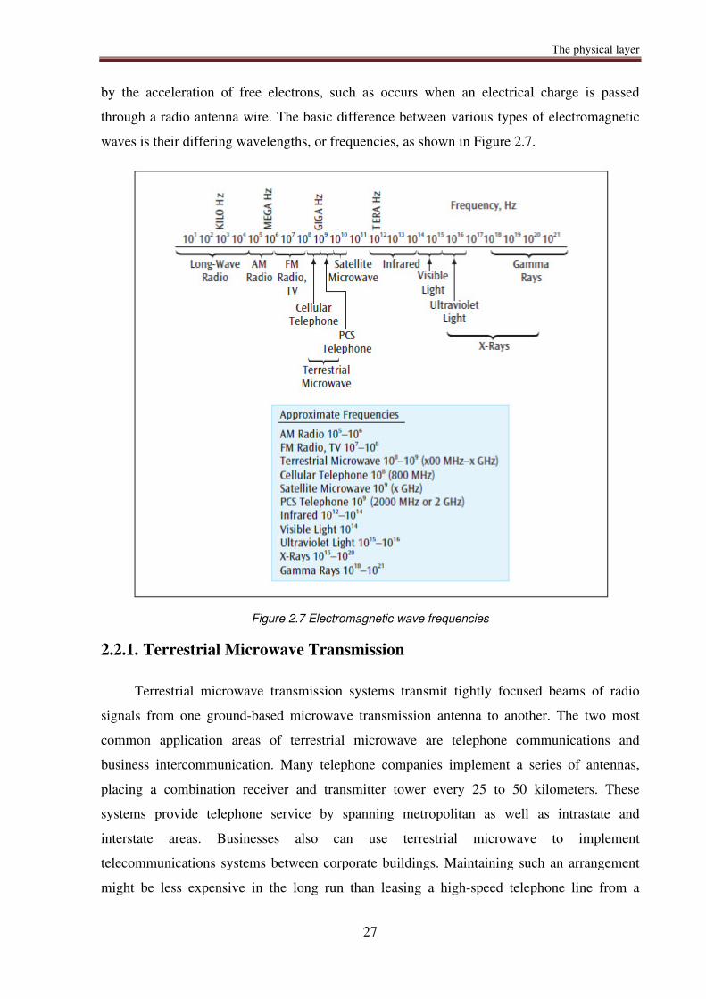
waves is their differing wavelengths, or frequencies, as shown in Figure 2.7.
Figure 2.7 Electromagnetic wave frequencies
2.2.1. Terrestrial Microwave Transmission
Terrestrial microwave transmission systems transmit tightly focused beams of radio
signals from one ground-based microwave transmission antenna to another. The two most
common application areas of terrestrial microwave are telephone communications and
business intercommunication. Many telephone companies implement a series of antennas,
placing a combination receiver and transmitter tower every 25 to 50 kilometers. These
systems provide telephone service by spanning metropolitan as well as intrastate and
interstate areas. Businesses also can use terrestrial microwave to implement
telecommunications systems between corporate buildings. Maintaining such an arrangement
might be less expensive in the long run than leasing a high-speed telephone line from a
The physical layer
28
telephone company, which requires an ongoing monthly payment. With terrestrial microwave,
once the system is purchased and installed, no telephone service fees are necessary.
Microwave transmissions do not follow the curvature of the Earth, nor do they pass
through solid objects, both of which limit their transmission distance. Microwave antennas
use line-of-sight transmission, which means that to receive and transmit a signal, each antenna
must be in sight of the next antenna. Many microwave antennas are located on top of free-
standing towers, and the typical distance between microwave towers is roughly 25 to 50
kilometers. The higher the tower, the farther the possible transmission distance. Thus, towers
located on hills or mountains, or atop tall buildings, can transmit signals farther than 50
kilometers. Another factor that limits transmission distance is the number of objects that
might obstruct the path of transmission signals. Buildings, hills, forests, and even heavy rain
and snowfall all interfere with the transmission of microwave signals. Considering these
limitations, the disadvantages of terrestrial microwave can include loss of signal strength
(attenuation) and interference from other signals (intermodulation), in addition to the costs of
either leasing the service or installing and maintaining the antennas.
2.2.2. Satellite Microwave Transmission
Satellite microwave transmission systems are similar to terrestrial microwave systems
except that the signal travels from a ground station on Earth to a satellite and back to another
ground station on Earth, thus achieving much greater distances than Earth-bound line-of-sight
transmissions.
One way of categorizing satellite systems is by how far the satellite is from the Earth.
The closer a satellite is to the Earth, the shorter the times required to send data to the
satellite—to uplink—and receive data from the satellite—to downlink. This transmission time
from ground station to satellite and back to ground station is called propagation delay. The
disadvantage to being closer to Earth is that the satellite must continuously circle the Earth to
remain in orbit. Thus, these satellites are constantly moving and eventually pass beyond the
horizon, ruining the line-of-sight transmission. Satellites that are always over the same point
on Earth can be used for long periods of high-speed data transfers.
Based on the range and the shape of the orbit the satellites are grouped in four
categories: low Earth orbit (LEO), middle Earth orbit (MEO), geosynchronous Earth orbit
(GEO. The LEO satellites are between 160Km and 2000 Km and are mainly used for Earth
observation. The MEO satellites are between 2000Km and 36000 Km and are used primarily
The physical layer
29
for global positioning system surface navigation applications. The GEO satellites are found
36,000 kilometers from the Earth and are always positioned over the same point on Earth
(somewhere over the equator). Their rotation period is equal to Earth’s period. They are
mainly used for communication purposes
Besides being classified as LEO, MEO and GEO, satellite systems can be categorized
into three basic topologies: bulk carrier facilities, multiplexed Earth stations, and single-user
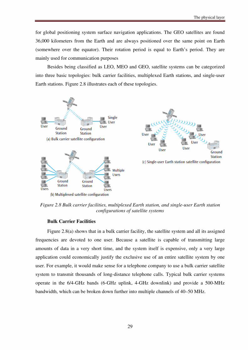
Earth stations. Figure 2.8 illustrates each of these topologies.
Figure 2.8 Bulk carrier facilities, multiplexed Earth station, and single-user Earth station
configurations of satellite systems
Bulk Carrier Facilities
Figure 2.8(a) shows that in a bulk carrier facility, the satellite system and all its assigned
frequencies are devoted to one user. Because a satellite is capable of transmitting large
amounts of data in a very short time, and the system itself is expensive, only a very large
application could economically justify the exclusive use of an entire satellite system by one
user. For example, it would make sense for a telephone company to use a bulk carrier satellite
system to transmit thousands of long-distance telephone calls. Typical bulk carrier systems
operate in the 6/4-GHz bands (6-GHz uplink, 4-GHz downlink) and provide a 500-MHz
bandwidth, which can be broken down further into multiple channels of 40–50 MHz.
The physical layer
30
Multiplexed Earth Station
In a multiplexed Earth station satellite system, the ground station accepts input from
multiple sources and in some fashion interweaves the data streams, either by assigning
different frequencies to different signals or by allowing different signals to take turns
transmitting. Figure 2.8(b) shows a diagram of how a typical multiplexed Earth station
satellite system operates. How does this type of satellite system satisfy the requests of users
and assign time slots? Each user could be asked in turn if he or she has data to transmit; but
because so much time could be lost during the asking process, this technique would not be
economically feasible. A first-come, first-served scenario, in which each user competes with
every other user, would also be an extremely inefficient design. The technique that seems to
work best for assigning access to multiplexed satellite systems is a reservation system. In a
reservation system, users place a reservation for future time slots. When the reserved time slot
arrives, the user transmits his or her data on the system. Two types of reservation systems
exist: centralized reservation and distributed reservation. In a centralized reservation system,
all reservations go to a central location, and that site handles the incoming requests. In a
distributed reservation system, no central site handles the reservations, but individual users
come to some agreement on the order of transmission.
Single-User Earth Station
In a single-user Earth station satellite system, each user employs his or her own ground
station to transmit data to the satellite. Figure 2.8(c) shows a typical single-user Earth station
satellite configuration. The Very Small Aperture Terminal (VSAT) system is an example of a
single-user Earth station satellite system with its own ground station and a small antenna (two
to six feet across). Among all the user ground stations is one master station that is typically
connected to a mainframe-like computer system. The ground stations communicate with the
mainframe computer via the satellite and master station. A VSAT end user needs an indoor
unit, which consists of a transceiver that interfaces the user’s computer system with an outside
satellite dish (the outdoor unit). This transceiver, which is small, sends signals to and receives
signals from a LEO satellite via the dish. VSAT is capable of handling data, voice, and video
signals over much of the Earth’s surface.
The physical layer
31
2.2.3. Bluetooth
The Bluetooth protocol—named after the Viking crusader Harald Bluetooth, who
unified Denmark and Norway in the tenth century—is a wireless technology that uses low-
power, short-range radio frequencies to communicate between two or more devices. More
precisely, Bluetooth uses the 2.45-GHz ISM (Industrial, Scientific, Medical) band and is
typically limited to distances less than 100m.
Bluetooth is capable of transmitting through nonmetallic objects, thus, a device that is
transmitting Bluetooth signals can be carried in a pocket, purse, or briefcase. Furthermore, it
is possible with Bluetooth to transfer data at reasonably high speeds. The first Bluetooth
standard was capable of data transfer rates up to roughly 700 kbps. The second standard
increased the data rate to a little more than 2 Mbps. The third reached the 3 Mbps limit and
could even go to a rate of up to 24 Mbit/s (however, not over the Bloetooth link itself, but
over an ad-hoc Wi-Fi link). Those three versions of Bluetooth had one big disadvantage, that
is the power consumption. As Internet of Things (IoT) become more and more spread, the
need of a low-power communication protocol force the implementation of the fourth version.
This one added a new mode called Bluetooth Low Energy (BLE) that has a lower data
transfer speed of only 1Mbit/s but with a considerable lower power consumption. The latest
version in use today is the fifth which, among other improvements, uses a maximum of 2
Mbit/s speed also with a low power consumption.
2.2.4. Wireless Local Area Networks
The first wireless local area network standard was introduced in 1997 by IEEE and is
called IEEE 802.11. IEEE 802.11 is capable of supporting data rates up to 2 Mbps and allows
wireless workstations up to roughly several hundred meters away to communicate with an
access point. This access point is the connection into the wired portion of the local area
network. In 1999, IEEE approved a new 11-Mbps protocol, IEEE 802.11b. This protocol is
also known as wireless fidelity (Wi-Fi) and transmits data in the 2.4-GHz frequency range.
802.11b was updated in 2003 with 802.11g. 802.11g transmits data at speeds up to 54 Mbps
(theoretical) and uses the same frequencies—2.4 GHz—as 802.11b.
A third wireless LAN protocol that was approved at the end of 2009 is IEEE 802.11n.
This standard is capable of supporting a 100-Mbps signal between wireless devices and uses
multiple antennas to support multiple independent data streams. IEEE 802.11n operates in
both 2.4-GHz and 5-GHz frequency ranges.

The physical layer
32
In December 2013 a new protocol named 803.11ac was published. It defines three data
streams of 433.3Mbps each, yielding a total of 1300 Mbps transfer rate.
All of these protocols—802.11b, 802.11g, 802.11n and 802.11ac—are now called Wi-
Fi.
Data and Signals
33
3. Data and Signals
3.1. Introduction
Information stored within computer systems and transferred over a communication
network can be divided into two categories: data and signals. Data is entities that convey
meaning within a computer system. Common examples of data include:
A computer file of names and addresses stored on a hard disk drive
The bits or individual elements of a movie stored on a DVD
The binary 1s and 0s of music stored on a CD or inside an iPod
The dots (pixels) of a photograph that has been digitized by a digital camera and stored
on a memory stick
The digits 0 through 9, which might represent some kind of sales figures for a business
In each of these examples, some kind of information has been electronically captured
and stored on some type of storage device.
If you want to transfer this data from one point to another, either via a physical wire or
through radio waves, the data must be converted into a signal. Signals are the electric or
electromagnetic impulses used to encode and transmit data. Common examples of signals
include:
A transmission of a telephone conversation over a telephone line
A live television news interview from Europe transmitted over a satellite system
A transmission of a term paper over the printer cable between a computer and a printer
The downloading of a Web page as it is transferred over the telephone line between
your Internet service provider and your home computer
In each of these examples, data, the static entity or tangible item, is transmitted over a
wire or an airwave in the form of a signal which is the dynamic entity or intangible item.
Some type of hardware device is necessary to convert the static data into a dynamic signal
ready for transmission and then convert the signal back to data at the receiving destination.
Data and Signals
34
Before examining the basic characteristics of data and signals and the conversion from
data to signal, however, let us explore the most important characteristic that data and signals
share.
Although data and signals are two different entities that have little in common, the one
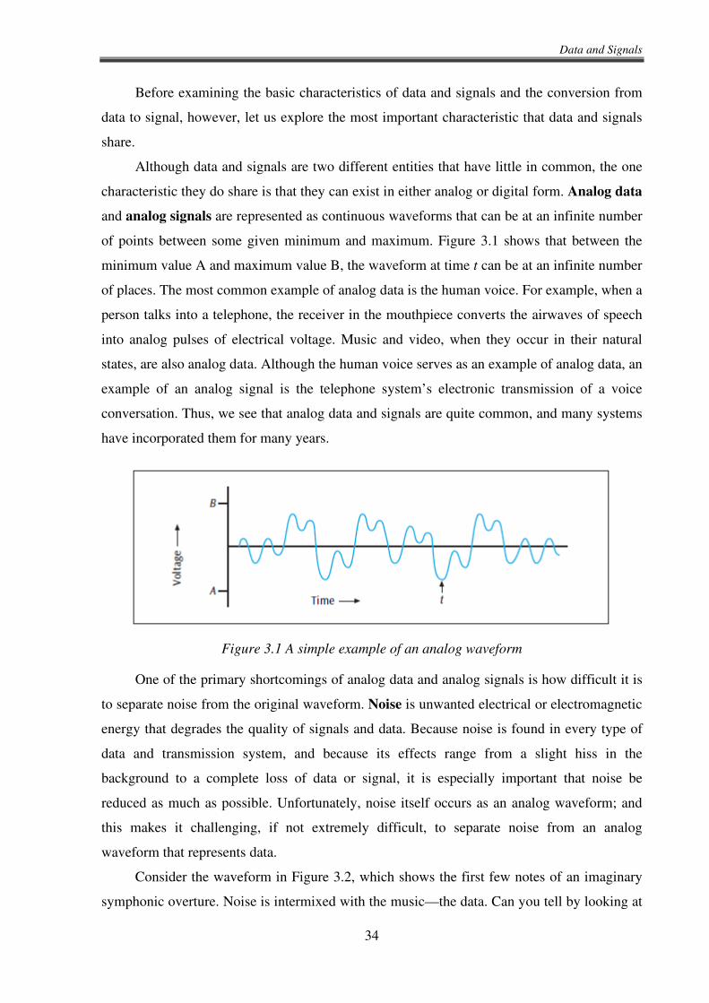
characteristic they do share is that they can exist in either analog or digital form. Analog data
and analog signals are represented as continuous waveforms that can be at an infinite number
of points between some given minimum and maximum. Figure 3.1 shows that between the
minimum value A and maximum value B, the waveform at time t can be at an infinite number
of places. The most common example of analog data is the human voice. For example, when a
person talks into a telephone, the receiver in the mouthpiece converts the airwaves of speech
into analog pulses of electrical voltage. Music and video, when they occur in their natural
states, are also analog data. Although the human voice serves as an example of analog data, an
example of an analog signal is the telephone system’s electronic transmission of a voice
conversation. Thus, we see that analog data and signals are quite common, and many systems
have incorporated them for many years.
Figure 3.1 A simple example of an analog waveform
One of the primary shortcomings of analog data and analog signals is how difficult it is
to separate noise from the original waveform. Noise is unwanted electrical or electromagnetic
energy that degrades the quality of signals and data. Because noise is found in every type of
data and transmission system, and because its effects range from a slight hiss in the
background to a complete loss of data or signal, it is especially important that noise be
reduced as much as possible. Unfortunately, noise itself occurs as an analog waveform; and
this makes it challenging, if not extremely difficult, to separate noise from an analog
waveform that represents data.
Consider the waveform in Figure 3.2, which shows the first few notes of an imaginary
symphonic overture. Noise is intermixed with the music—the data. Can you tell by looking at

Data and Signals
35
the figure what is the data and what is the noise? Although this example might border on the
extreme, it demonstrates that noise and analog data can appear to be similar.
Figure 3.2 The waveform of a symphonic overture with noise
The performance of a record player provides another example of noise interfering with
data. Many people have collections of albums, which produce pops, hisses, and clicks when
played; albums sometimes even skip. Is it possible to create a device that filters out the pops,
hisses, and clicks from a record album without ruining the original data, the music? Various
devices were created during the 1960s and 1970s to perform these kinds of filtering, but only
the devices that removed hisses were (relatively speaking) successful. Filtering devices that
removed the pops and clicks also tended to remove parts of the music. Filters now exist that
can fairly effectively remove most forms of noise from analog recordings; but they are,
interestingly, digital—not analog— devices. Even more interestingly, some people download
software from the Internet that lets them insert clicks and pops into digital music to make it
sound old-fashioned (in other words, as though it were being played from a record album).
Another example of noise interfering with an analog signal is the hiss and static you
hear when you are talking on the telephone. Often the background noise is so slight that most
people do not notice it. Occasionally, however, the noise rises to such a level that it interferes
with the conversation. Yet another common example of noise interference occurs when you
listen to an AM radio station during an electrical storm. The radio signal crackles with every
lightning strike within the area.
Digital data and digital signals are composed of a discrete or fixed number of values,
rather than a continuous or infinite number of values. Digital data takes on the form of binary
1s and 0s. But digital signals are more complex. To keep the discussion as simple as possible
only the most simple type of digital signal is presented: the “square wave.” These square
waves are relatively simple patterns of high and low voltages. In the example shown in Figure

Data and Signals
36
3.3, the digital square wave takes on only two discrete values: a high voltage (such as 5 volts)
and a low voltage (such as 0 volts).
Figure 3.3 A simple example of a digital waveform
What happens when you introduce noise into digital signals? As stated earlier, noise has
the properties of an analog waveform and, thus, can occupy an infinite range of values; digital
waveforms occupy only a finite range of values. When you combine analog noise with a
digital waveform, it is fairly easy to separate the original digital waveform from the noise.
Figure 3.4 shows a digital signal (square wave) with some noise.
Figure 3.4 A digital signal with some noise introduced
If the amount of noise remains small enough that the original digital waveform can still
be interpreted, then the noise can be filtered out, thereby leaving the original waveform. In the
simple example in Figure 3.4, as long as you can tell a high part of the waveform from a low
part, you can still recognize the digital waveform. If, however, the noise becomes so great that
it is no longer possible to distinguish a high from a low, as shown in Figure 3.5, then the noise
has taken over the signal and you can no longer understand this portion of the waveform.
Data and Signals
37
Figure 3.5 A digital waveform with noise so great that you can no longer recognize the
original waveform
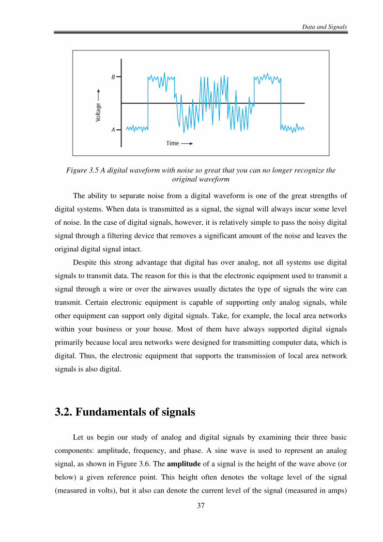
The ability to separate noise from a digital waveform is one of the great strengths of
digital systems. When data is transmitted as a signal, the signal will always incur some level
of noise. In the case of digital signals, however, it is relatively simple to pass the noisy digital
signal through a filtering device that removes a significant amount of the noise and leaves the
original digital signal intact.
Despite this strong advantage that digital has over analog, not all systems use digital
signals to transmit data. The reason for this is that the electronic equipment used to transmit a
signal through a wire or over the airwaves usually dictates the type of signals the wire can
transmit. Certain electronic equipment is capable of supporting only analog signals, while
other equipment can support only digital signals. Take, for example, the local area networks
within your business or your house. Most of them have always supported digital signals
primarily because local area networks were designed for transmitting computer data, which is
digital. Thus, the electronic equipment that supports the transmission of local area network
signals is also digital.
3.2. Fundamentals of signals
Let us begin our study of analog and digital signals by examining their three basic
components: amplitude, frequency, and phase. A sine wave is used to represent an analog
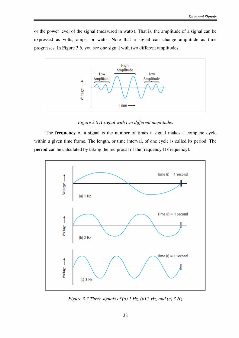
signal, as shown in Figure 3.6. The amplitude of a signal is the height of the wave above (or
below) a given reference point. This height often denotes the voltage level of the signal
(measured in volts), but it also can denote the current level of the signal (measured in amps)
Data and Signals
38
or the power level of the signal (measured in watts). That is, the amplitude of a signal can be
expressed as volts, amps, or watts. Note that a signal can change amplitude as time
progresses. In Figure 3.6, you see one signal with two different amplitudes.
Figure 3.6 A signal with two different amplitudes
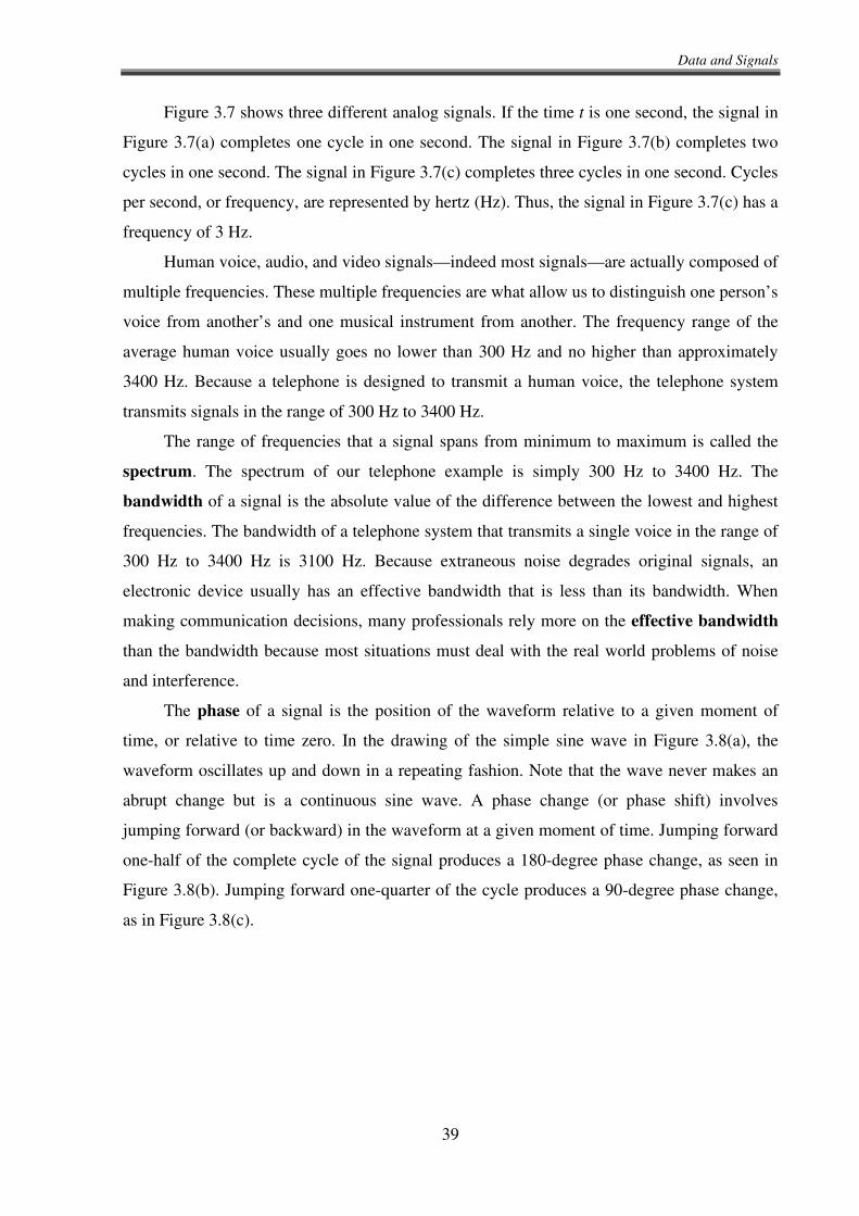
The frequency of a signal is the number of times a signal makes a complete cycle
within a given time frame. The length, or time interval, of one cycle is called its period. The
period can be calculated by taking the reciprocal of the frequency (1/frequency).
Figure 3.7 Three signals of (a) 1 Hz, (b) 2 Hz, and (c) 3 Hz
Data and Signals
39
Figure 3.7 shows three different analog signals. If the time t is one second, the signal in
Figure 3.7(a) completes one cycle in one second. The signal in Figure 3.7(b) completes two
cycles in one second. The signal in Figure 3.7(c) completes three cycles in one second. Cycles
per second, or frequency, are represented by hertz (Hz). Thus, the signal in Figure 3.7(c) has a
frequency of 3 Hz.
Human voice, audio, and video signals—indeed most signals—are actually composed of
multiple frequencies. These multiple frequencies are what allow us to distinguish one person’s
voice from another’s and one musical instrument from another. The frequency range of the
average human voice usually goes no lower than 300 Hz and no higher than approximately
3400 Hz. Because a telephone is designed to transmit a human voice, the telephone system
transmits signals in the range of 300 Hz to 3400 Hz.
The range of frequencies that a signal spans from minimum to maximum is called the
spectrum. The spectrum of our telephone example is simply 300 Hz to 3400 Hz. The
bandwidth of a signal is the absolute value of the difference between the lowest and highest
frequencies. The bandwidth of a telephone system that transmits a single voice in the range of
300 Hz to 3400 Hz is 3100 Hz. Because extraneous noise degrades original signals, an
electronic device usually has an effective bandwidth that is less than its bandwidth. When
making communication decisions, many professionals rely more on the effective bandwidth
than the bandwidth because most situations must deal with the real world problems of noise
and interference.
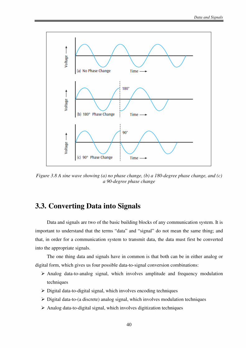
The phase of a signal is the position of the waveform relative to a given moment of
time, or relative to time zero. In the drawing of the simple sine wave in Figure 3.8(a), the
waveform oscillates up and down in a repeating fashion. Note that the wave never makes an
abrupt change but is a continuous sine wave. A phase change (or phase shift) involves
jumping forward (or backward) in the waveform at a given moment of time. Jumping forward
one-half of the complete cycle of the signal produces a 180-degree phase change, as seen in
Figure 3.8(b). Jumping forward one-quarter of the cycle produces a 90-degree phase change,
as in Figure 3.8(c).
Data and Signals
40
Figure 3.8 A sine wave showing (a) no phase change, (b) a 180-degree phase change, and (c)
a 90-degree phase change
3.3. Converting Data into Signals
Data and signals are two of the basic building blocks of any communication system. It is
important to understand that the terms “data” and “signal” do not mean the same thing; and
that, in order for a communication system to transmit data, the data must first be converted
into the appropriate signals.
The one thing data and signals have in common is that both can be in either analog or
digital form, which gives us four possible data-to-signal conversion combinations:
Analog data-to-analog signal, which involves amplitude and frequency modulation
techniques
Digital data-to-digital signal, which involves encoding techniques
Digital data-to-(a discrete) analog signal, which involves modulation techniques
Analog data-to-digital signal, which involves digitization techniques
Data and Signals
41
Each of these four combinations occurs quite frequently in communication systems, and
each has unique applications and properties, which are shown in Table 3-1.
Table 3-1 Four combinations of data and signals
Data Signal Encoding or Conversion
Technique
Common
Devices
Common
Systems
Analog Analog Amplitude modulation Frequency modulation Phase modulation
Radio tuner TV tuner
Telephone AM and FM radio Broadcast TV Analog Cable TV
Digital Digital NRZ-L NRZ-I Manchester Differential Manchester Bipolar-AMI 4B/5B
Digital encoder Local area networks Telephone systems
Digital (Discrete) Analog
Amplitude shift keying Frequency shift keying Phase shift keying Quadrature amplitude modulation
Modem Dial-up Internet access DSL Cable modems Digital Broadcast TV
Analog Digital Pulse code modulation Delta modulation
Codec Telephone systems Music systems
Converting analog data to analog signals is fairly common. The conversion is performed
by modulation techniques and is found in systems such as telephones, AM radio, and FM
radio. Converting digital data to digital signals is relatively straightforward and involves
numerous digital encoding techniques. With this technique, binary 1s and 0s are converted to
varying types of on and off voltage levels. The local area network is one of the most common
examples of a system that uses this type of conversion. Converting digital data to (discrete)
analog signals requires some form of a modem. Once again we are converting the binary 1s
and 0s to another form; but unlike converting digital data to digital signals, the conversion of
digital data to discrete analog signals involves more complex forms of analog signals that take
on a discrete, or fixed, number of levels. Finally, converting analog data to digital signals is
generally called digitization. Telephone systems and music systems are two common
examples of digitization. When your voice signal travels from your home and reaches a
telephone company’s switching center, it is digitized. Likewise, music and video are digitized
before they can be recorded on a CD or DVD.

Data and Signals
42
3.3.1. Transmitting analog data with analog signals
Of the four combinations of data and signals, the analog data-to-analog signal
conversion is probably the simplest to comprehend. This is because the data is an analog
waveform that is simply being transformed to another analog waveform, the signal, for
transmission. The basic operation performed is modulation. Modulation is the process of
sending data over a signal by varying either its amplitude, frequency, or phase. Land-line
telephones (the local loop only), AM radio, FM radio, and broadcast television are the most
common examples of analog data-to-analog signal conversion.
Figure 3.9 An audio waveform modulated onto a carrier frequency using amplitude
modulation
Consider Figure 3.9, which shows AM radio as an example. The audio data generated
by the radio station might appear like the first sine wave shown in the figure. To convey this
analog data, the station uses a carrier wave signal, like that shown in Figure 3.9(b). In the
modulation process, the original audio waveform and the carrier wave are essentially added
together to produce the third waveform. Note how the dotted lines superimposed over the
third waveform follow the same outline as the original audio waveform. Here, the original
Data and Signals
43
audio data has been modulated onto a particular carrier frequency (the frequency at which you
set the dial to tune in a station) using amplitude modulation—hence, the name AM radio.
Frequency modulation also can be used in similar ways to modulate analog data onto an
analog signal, and it yields FM radio.
3.3.2. Transmitting digital data with digital signals
To transmit digital data using digital signals, the 1s and 0s of the digital data must be
converted to the proper physical form that can be transmitted over a wire or an airwave. Thus,
if one wishes to transmit a data value of 1, this could be done by transmitting a positive
voltage on the medium. If a data value of 0 must be transmitted, then a zero voltage could be
sent. The opposite scheme can also be used: a data value of 0 is positive voltage and a data
value of 1 is a zero voltage. Digital encoding schemes like this are used to convert the 0s and
1s of digital data into the appropriate transmission form. In the following six digital encoding
schemes, that are representative, are presented: NRZ-L, NRZI, Manchester, differential
Manchester, bipolar-AMI, and 4B/5B.
Non-return to Zero Digital Encoding Schemes
The non-return to zero-level (NRZ-L) digital encoding scheme transmits 1s as zero
voltages and 0s as positive voltages. The NRZ-L encoding scheme is simple to generate and
inexpensive to implement in hardware. Figure 3.10(a) shows an example of the NRZ-L
scheme.
The second digital encoding scheme, shown in Figure 3.10(b), is non-return to zero
inverted (NRZI). This encoding scheme has a voltage change at the beginning of a 1 and no
voltage change at the beginning of a 0. A fundamental difference exists between NRZ-L and
NRZI. With NRZ-L, the receiver must check the voltage level for each bit to determine
whether the bit is a 0 or a 1. With NRZI, the receiver must check whether there is a change at
the beginning of the bit to determine if it is a 0 or a 1.
An inherent problem with the NRZ-L and NRZI digital encoding schemes is that long
sequences of 0s in the data produce a signal that never changes. Often the receiver looks for
signal changes so that it can synchronize its reading of the data with the actual data pattern. If
a long string of 0s is transmitted and the signal does not change, how can the receiver tell
when one bit ends and the next bit begins? One potential solution is to install in the receiver
an internal clock that knows when to look for each successive bit. But what if the receiver has
a different clock from the one the transmitter used to generate the signals? Who is to say that
Data and Signals
44
these two clocks keep the same time? A more accurate system would generate a signal that
has a change for each and every bit. If the receiver could count on each bit having some form
of signal change, then it could stay synchronized with the incoming data stream.
Figure 3.10 Examples of five digital encoding schemes
Data and Signals
45
Manchester Digital Encoding Schemes
The Manchester class of digital encoding schemes ensures that each bit has some type
of signal change, and thus solves the synchronization problem. Shown in Figure 3.10(c), the
Manchester encoding scheme has the following properties: To transmit a 1, the signal
changes from low to high in the middle of the interval, and to transmit a 0, the signal changes
from high to low in the middle of the interval. Note that the transition is always in the middle,
a 1 is a low-to-high transition, and a 0 is a high-to-low transition. Thus, if the signal is
currently low and the next bit to transmit is a 0, the signal must move from low to high at the
beginning of the interval so that it can do the high-to-low transition in the middle.
The differential Manchester digital encoding scheme was used in a now extinct form
of local area network (token ring) but still exists in a number of unique applications. It is
similar to the Manchester scheme in that there is always a transition in the middle of the
interval. But unlike the Manchester code, the direction of this transition in the middle does not
differentiate between a 0 or a 1. Instead, if there is a transition at the beginning of the interval,
then a 0 is being transmitted. If there is no transition at the beginning of the interval, then a 1
is being transmitted. Because the receiver must watch the beginning of the interval to
determine the value of the bit, the differential Manchester is similar to the NRZI scheme (in
this one respect). Figure 3.10(d) shows an example of differential Manchester encoding.
The Manchester schemes have an advantage over the NRZ schemes: In the Manchester
schemes, there is always a transition in the middle of a bit. Thus, the receiver can expect a
signal change at regular intervals and can synchronize itself with the incoming bit stream. The
Manchester encoding schemes are called self-clocking because the occurrence of a regular
transition is similar to seconds ticking on a clock.
The big disadvantage of the Manchester schemes is that roughly half the time there will
be two transitions during each bit. For example, if the differential Manchester encoding
scheme is used to transmit a series of 0s, then the signal has to change at the beginning of
each bit, as well as change in the middle of each bit. Thus, for each data value 0, the signal
changes twice. The number of times a signal changes value per second is called the baud
rate, or simply baud.
In Figure 3.11, a series of binary 0s is transmitted using the differential Manchester
encoding scheme. Note that the signal changes twice for each bit. After one second, the signal
has changed 10 times. Therefore, the baud rate is 10. During that same time period, only 5 bits
were transmitted. The data rate, measured in bits per second (bps), is 5, which in this case is
one-half the baud rate. Many individuals mistakenly equate baud rate to bps (or data rate).
Data and Signals
46
Under some circumstances, the baud rate might equal the bps, such as in the NRZ-L or NRZI
encoding schemes shown in. In these, there is at most one signal change for each bit
transmitted. But with schemes such as the Manchester codes, the baud rate is not equal to the
bps.
Figure 3.11 Transmitting five binary 0s using differential Manchester encoding
Why does it matter that some encoding schemes have a baud rate twice the bps?
Because the Manchester codes have a baud rate that is twice the bps, and the NRZ-L and
NRZI codes have a baud rate that is equal to the bps, hardware that generates a Manchester-
encoded signal must work twice as fast as hardware that generates an NRZ-encoded signal. If
100 million 0s per second are transmitted using differential Manchester encoding, the signal
must change 200 million times per second (as opposed to 100 million times per second with
NRZ encoding). As with most things in life, you do not get something for nothing. Hardware
or software that handles the Manchester encoding schemes is more elaborate and more costly
than the hardware or software that handles the NRZ encoding schemes. More importantly,
signals that change at a higher rate of speed are more susceptible to noise and errors.
Bipolar-AMI (alternate mark inversion) Encoding Scheme
The bipolar-AMI (alternate mark inversion) encoding scheme is unique among all the
encoding schemes seen thus far because it uses three voltage levels. When a device transmits
a binary 0, a zero voltage is transmitted. When the device transmits a binary 1, either a
positive voltage or a negative voltage is transmitted. Which of these is transmitted depends on
the binary 1 value that was last transmitted. For example, if the last binary 1 transmitted a
positive voltage, then the next binary 1 will transmit a negative voltage. Likewise, if the last
binary 1 transmitted a negative voltage, then the next binary 1 will transmit a positive voltage.
The bipolar scheme has two obvious disadvantages. First, as you can see in Figure 3.10(e), we
have the long-string-of-0s synchronization problem again, as we had with the NRZ schemes.
Second, the hardware must now be capable of generating and recognizing negative voltages
Data and Signals
47
as well as positive voltages. On the other hand, the primary advantage of a bipolar scheme is
that when all the voltages are added together after a long transmission, there should be a total
voltage of zero. That is, the positive and negative voltages essentially cancel each other out.
This type of zero voltage sum can be useful in certain types of electronic systems.
4B/5B Digital Encoding Scheme
The Manchester encoding schemes solve the synchronization problem but are relatively
inefficient because they have a baud rate that is twice the bps. The 4B/5B scheme tries to
satisfy the synchronization problem and avoid the “baud equals two times the bps” problem.
The 4B/5B encoding scheme takes 4 bits of data, converts the 4 bits into a unique 5-bit
sequence, and encodes the 5 bits using NRZI.
Figure 3.12 The 4B/5B digital encoding scheme
. The first step the hardware performs in generating the 4B/5B code is to convert 4-bit
quantities of the original data into new 5-bit quantities. Using 5 bits (or five 0s and 1s) to
represent one value yields 32 potential combinations (25 = 32). Of these possibilities, only 16
combinations are used, so that no code has three or more consecutive 0s. This way, if the
transmitting device transmits the 5-bit quantities using NRZI encoding, there will never be
Data and Signals
48
more than two 0s in a row transmitted (unless one 5-bit character ends with 00, and the next
5-bit character begins with a 0). If you never transmit more than two 0s in a row using NRZI
encoding, then you will never have a long period in which there is no signal transition. Figure
3.12 shows the 4B/5B code in detail.
How does the 4B/5B code work? Let us say, for example, that the next 4 bits in a data
stream to be transmitted are 0000, which, you can see, has a string of consecutive zeros and
therefore would create a signal that does not change. Looking at the first column in Figure
3.12, we see that 4B/5B encoding replaces 0000 with 11110. Note that 11110, like all the 5-
bit codes in the second column of Figure 3.12, does not have more than two consecutive
zeros. Having replaced 0000 with 11110, the hardware will now transmit 11110. Because this
5-bit code is transmitted using NRZI, the baud rate equals the bps and, thus, is more efficient.
Unfortunately, converting a 4-bit code to a 5-bit code creates a 20 percent overhead (one extra
bit). Compare that to a Manchester code, in which the baud rate can be twice the bps and thus
yield a 100 percent overhead. Clearly, a 20 percent overhead is better than a 100 percent
overhead. Many of the newer digital encoding systems that use fiber-optic cable also use
techniques that are quite similar to 4B/5B.
3.3.3. Transmitting digital data with discrete analog signals
The technique of converting digital data to an analog signal is also an example of
modulation. But in this type of modulation, the analog signal takes on a discrete number of
signal levels. It could be as simple as two signal levels or something more complex as 256
levels as is used with digital television signals. The receiver then looks specifically for these
unique signal levels. Thus, even though they are fundamentally analog signals, they operate
with a discrete number of levels, much like a digital signal from the previous section. So to
avoid confusion, we’ll label them discrete analog signals. Let’s examine a number of these
discrete modulation techniques beginning with the simpler techniques (shift keying) and
ending with the more complex techniques used for systems such as digital television signals—
quadrature amplitude modulation.
Amplitude Shift Keying
The simplest modulation technique is amplitude shift keying. As shown in Figure 3.13,
a data value of 1 and a data value of 0 are represented by two different amplitudes of a signal.
For example, the higher amplitude could represent a 1, while the lower amplitude (or zero
Data and Signals
49
amplitude) could represent a 0. Note that during each bit period, the amplitude of the signal is
constant.
Figure 3.13 A simple example of amplitude shift keying
Amplitude shift keying is not restricted to two possible amplitude levels. For example,
we could create an amplitude shift keying technique that incorporates four different amplitude
levels, as shown in Figure 3.14. Each of the four different amplitude levels would represent 2
bits. You might recall that when counting in binary, 2 bits yield four possible combinations:
00, 01, 10, and 11. Thus, every time the signal changes (every time the amplitude changes), 2
bits are transmitted. As a result, the data rate (bps) is twice the baud rate. This is the opposite
of a Manchester code in which the data rate is one-half the baud rate. A system that transmits
2 bits per signal change is more efficient than one that requires two signal changes for every
bit.
Figure 3.14 Amplitude shift keying using four different amplitude levels
Amplitude shift keying has a weakness: It is susceptible to sudden noise impulses such
as the static charges created by a lightning storm. When a signal is disrupted by a large static
discharge, the signal experiences significant increases in amplitude. For this reason, and
Data and Signals
50
because it is difficult to accurately distinguish among more than just a few amplitude levels,
amplitude shift keying is one of the least efficient encoding techniques and is not used on
systems that require a high data transmission rate. When transmitting data over standard
telephone lines, amplitude shift keying typically does not exceed 1200 bps.
Frequency Shift Keying
Frequency shift keying uses two different frequency ranges to represent data values of 0
and 1, as shown in Figure 3.15. For example, the lower frequency signal might represent a 1,
while the higher frequency signal might represent a 0. During each bit period, the frequency
of the signal is constant.
Figure 3.15 Simple example of frequency shift keying
Unlike amplitude shift keying, frequency shift keying does not have a problem with
sudden noise spikes that can cause loss of data. Nonetheless, frequency shift keying is not
perfect. It is subject to intermodulation distortion, a phenomenon that occurs when the
frequencies of two or more signals mix together and create new frequencies. Thus, like
amplitude shift keying, frequency shift keying is not used on systems that require a high data
rate.
Phase Shift Keying
A third modulation technique is phase shift keying. Phase shift keying represents 0s and
1s by different changes in the phase of a waveform. For example, a 0 could be no phase
change, while a 1 could be a phase change of 180 degrees, as shown in Figure 3.16.
Phase changes are not affected by amplitude changes, nor are they affected by
intermodulation distortions. Thus, phase shift keying is less susceptible to noise and can be
used at higher frequencies. Phase shift keying is so accurate that the signal transmitter can
increase efficiency by introducing multiple phase shift angles.
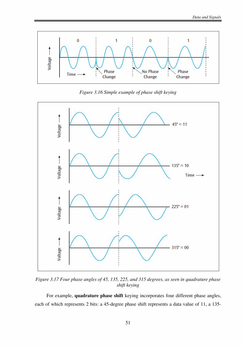
Data and Signals
51
Figure 3.16 Simple example of phase shift keying
Figure 3.17 Four phase angles of 45, 135, 225, and 315 degrees, as seen in quadrature phase
shift keying
For example, quadrature phase shift keying incorporates four different phase angles,
each of which represents 2 bits: a 45-degree phase shift represents a data value of 11, a 135-
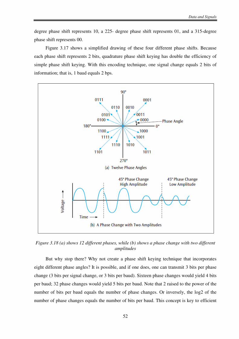
Data and Signals
52
degree phase shift represents 10, a 225- degree phase shift represents 01, and a 315-degree
phase shift represents 00.
Figure 3.17 shows a simplified drawing of these four different phase shifts. Because
each phase shift represents 2 bits, quadrature phase shift keying has double the efficiency of
simple phase shift keying. With this encoding technique, one signal change equals 2 bits of
information; that is, 1 baud equals 2 bps.
Figure 3.18 (a) shows 12 different phases, while (b) shows a phase change with two different
amplitudes
But why stop there? Why not create a phase shift keying technique that incorporates
eight different phase angles? It is possible, and if one does, one can transmit 3 bits per phase
change (3 bits per signal change, or 3 bits per baud). Sixteen phase changes would yield 4 bits
per baud; 32 phase changes would yield 5 bits per baud. Note that 2 raised to the power of the
number of bits per baud equals the number of phase changes. Or inversely, the log2 of the
number of phase changes equals the number of bits per baud. This concept is key to efficient
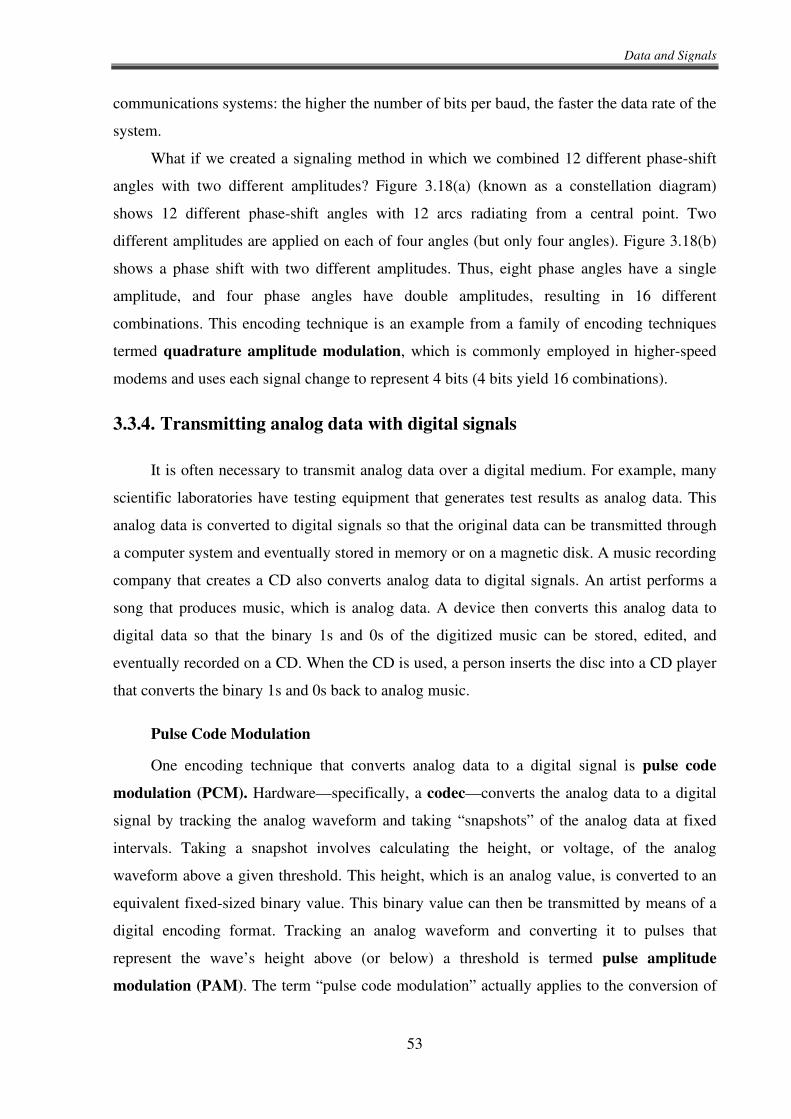
Data and Signals
53
communications systems: the higher the number of bits per baud, the faster the data rate of the
system.
What if we created a signaling method in which we combined 12 different phase-shift
angles with two different amplitudes? Figure 3.18(a) (known as a constellation diagram)
shows 12 different phase-shift angles with 12 arcs radiating from a central point. Two
different amplitudes are applied on each of four angles (but only four angles). Figure 3.18(b)
shows a phase shift with two different amplitudes. Thus, eight phase angles have a single
amplitude, and four phase angles have double amplitudes, resulting in 16 different
combinations. This encoding technique is an example from a family of encoding techniques
termed quadrature amplitude modulation, which is commonly employed in higher-speed
modems and uses each signal change to represent 4 bits (4 bits yield 16 combinations).
3.3.4. Transmitting analog data with digital signals
It is often necessary to transmit analog data over a digital medium. For example, many
scientific laboratories have testing equipment that generates test results as analog data. This
analog data is converted to digital signals so that the original data can be transmitted through
a computer system and eventually stored in memory or on a magnetic disk. A music recording
company that creates a CD also converts analog data to digital signals. An artist performs a
song that produces music, which is analog data. A device then converts this analog data to
digital data so that the binary 1s and 0s of the digitized music can be stored, edited, and
eventually recorded on a CD. When the CD is used, a person inserts the disc into a CD player
that converts the binary 1s and 0s back to analog music.
Pulse Code Modulation
One encoding technique that converts analog data to a digital signal is pulse code
modulation (PCM). Hardware—specifically, a codec—converts the analog data to a digital
signal by tracking the analog waveform and taking “snapshots” of the analog data at fixed
intervals. Taking a snapshot involves calculating the height, or voltage, of the analog
waveform above a given threshold. This height, which is an analog value, is converted to an
equivalent fixed-sized binary value. This binary value can then be transmitted by means of a
digital encoding format. Tracking an analog waveform and converting it to pulses that
represent the wave’s height above (or below) a threshold is termed pulse amplitude
modulation (PAM). The term “pulse code modulation” actually applies to the conversion of
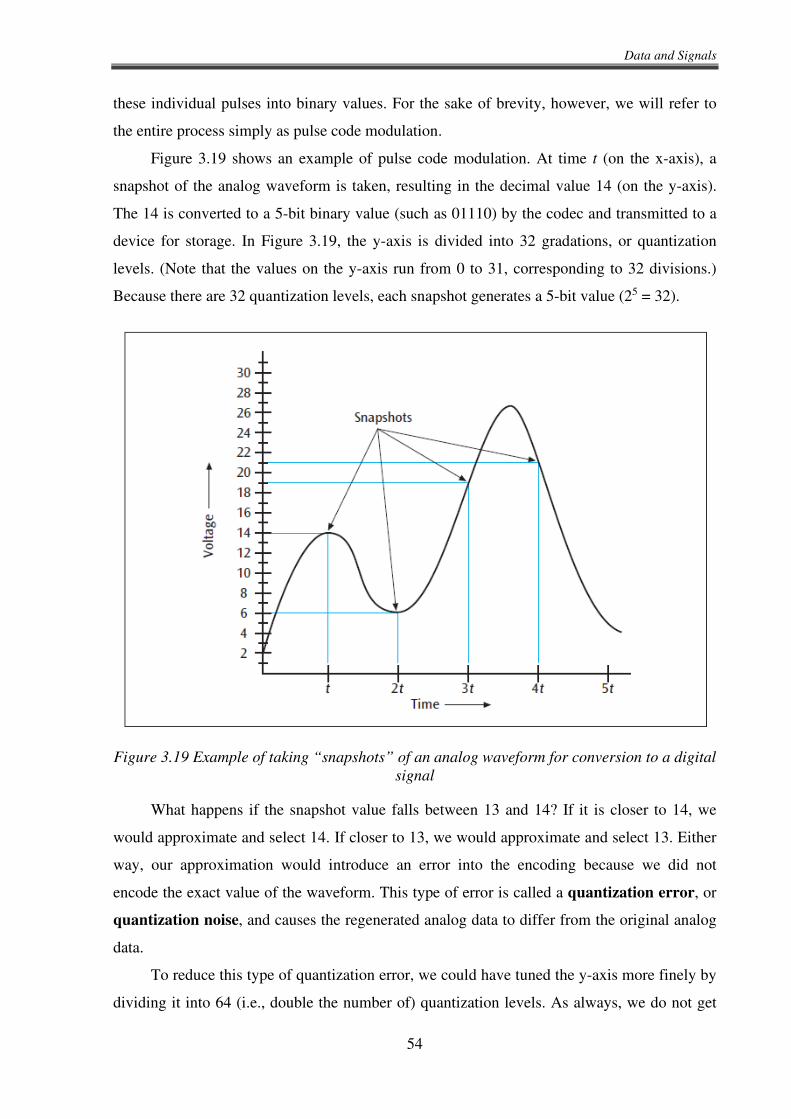
Data and Signals
54
these individual pulses into binary values. For the sake of brevity, however, we will refer to
the entire process simply as pulse code modulation.
Figure 3.19 shows an example of pulse code modulation. At time t (on the x-axis), a
snapshot of the analog waveform is taken, resulting in the decimal value 14 (on the y-axis).
The 14 is converted to a 5-bit binary value (such as 01110) by the codec and transmitted to a
device for storage. In Figure 3.19, the y-axis is divided into 32 gradations, or quantization
levels. (Note that the values on the y-axis run from 0 to 31, corresponding to 32 divisions.)
Because there are 32 quantization levels, each snapshot generates a 5-bit value (25 = 32).
Figure 3.19 Example of taking “snapshots” of an analog waveform for conversion to a digital
signal
What happens if the snapshot value falls between 13 and 14? If it is closer to 14, we
would approximate and select 14. If closer to 13, we would approximate and select 13. Either
way, our approximation would introduce an error into the encoding because we did not
encode the exact value of the waveform. This type of error is called a quantization error, or
quantization noise, and causes the regenerated analog data to differ from the original analog
data.
To reduce this type of quantization error, we could have tuned the y-axis more finely by
dividing it into 64 (i.e., double the number of) quantization levels. As always, we do not get
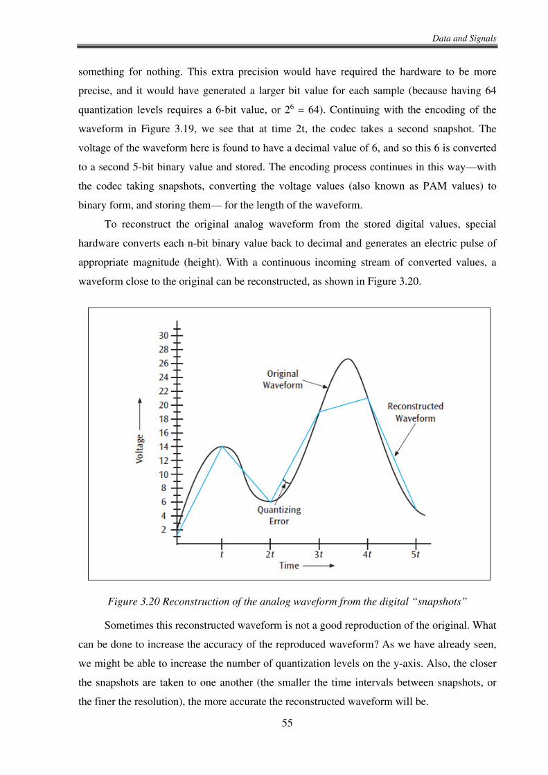
Data and Signals
55
something for nothing. This extra precision would have required the hardware to be more
precise, and it would have generated a larger bit value for each sample (because having 64
quantization levels requires a 6-bit value, or 26 = 64). Continuing with the encoding of the
waveform in Figure 3.19, we see that at time 2t, the codec takes a second snapshot. The
voltage of the waveform here is found to have a decimal value of 6, and so this 6 is converted
to a second 5-bit binary value and stored. The encoding process continues in this way—with
the codec taking snapshots, converting the voltage values (also known as PAM values) to
binary form, and storing them— for the length of the waveform.
To reconstruct the original analog waveform from the stored digital values, special
hardware converts each n-bit binary value back to decimal and generates an electric pulse of
appropriate magnitude (height). With a continuous incoming stream of converted values, a
waveform close to the original can be reconstructed, as shown in Figure 3.20.
Figure 3.20 Reconstruction of the analog waveform from the digital “snapshots”
Sometimes this reconstructed waveform is not a good reproduction of the original. What
can be done to increase the accuracy of the reproduced waveform? As we have already seen,
we might be able to increase the number of quantization levels on the y-axis. Also, the closer
the snapshots are taken to one another (the smaller the time intervals between snapshots, or
the finer the resolution), the more accurate the reconstructed waveform will be.
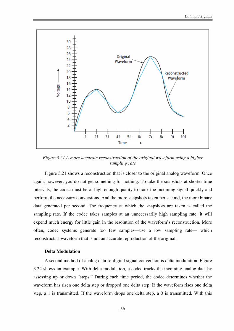
Data and Signals
56
Figure 3.21 A more accurate reconstruction of the original waveform using a higher
sampling rate
Figure 3.21 shows a reconstruction that is closer to the original analog waveform. Once
again, however, you do not get something for nothing. To take the snapshots at shorter time
intervals, the codec must be of high enough quality to track the incoming signal quickly and
perform the necessary conversions. And the more snapshots taken per second, the more binary
data generated per second. The frequency at which the snapshots are taken is called the
sampling rate. If the codec takes samples at an unnecessarily high sampling rate, it will
expend much energy for little gain in the resolution of the waveform’s reconstruction. More
often, codec systems generate too few samples—use a low sampling rate— which
reconstructs a waveform that is not an accurate reproduction of the original.
Delta Modulation
A second method of analog data-to-digital signal conversion is delta modulation. Figure
3.22 shows an example. With delta modulation, a codec tracks the incoming analog data by
assessing up or down “steps.” During each time period, the codec determines whether the
waveform has risen one delta step or dropped one delta step. If the waveform rises one delta
step, a 1 is transmitted. If the waveform drops one delta step, a 0 is transmitted. With this
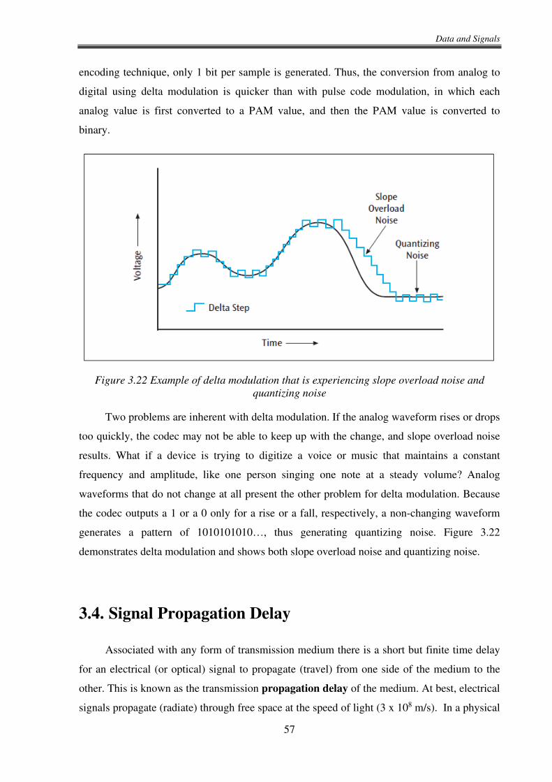
Data and Signals
57
encoding technique, only 1 bit per sample is generated. Thus, the conversion from analog to
digital using delta modulation is quicker than with pulse code modulation, in which each
analog value is first converted to a PAM value, and then the PAM value is converted to
binary.
Figure 3.22 Example of delta modulation that is experiencing slope overload noise and
quantizing noise
Two problems are inherent with delta modulation. If the analog waveform rises or drops
too quickly, the codec may not be able to keep up with the change, and slope overload noise
results. What if a device is trying to digitize a voice or music that maintains a constant
frequency and amplitude, like one person singing one note at a steady volume? Analog
waveforms that do not change at all present the other problem for delta modulation. Because
the codec outputs a 1 or a 0 only for a rise or a fall, respectively, a non-changing waveform
generates a pattern of 1010101010…, thus generating quantizing noise. Figure 3.22
demonstrates delta modulation and shows both slope overload noise and quantizing noise.
3.4. Signal Propagation Delay
Associated with any form of transmission medium there is a short but finite time delay
for an electrical (or optical) signal to propagate (travel) from one side of the medium to the
other. This is known as the transmission propagation delay of the medium. At best, electrical
signals propagate (radiate) through free space at the speed of light (3 x 10⁸ m/s). In a physical

Data and Signals
58
transmission medium, such as twisted pair wire or coaxial cable, however, the speed of
propagation is a fraction of this figure. Typically, it is in the region of 2 x 10⁸ m/s; that is, a
signal will take 0.5 x 10⁻⁸ s to travel 1 m of the medium. Although this may seem
insignificant, in some situations the resulting delay is important.
As will be seen in subsequent chapters, data are normally transmitted in blocks (also
known as frames) of bits and, on receipt of a block, an acknowledgement of correct (or
otherwise) receipt is returned to the sender. An important parameter associated with a data
link, therefore, is the round-trip delay associated with the link; that is, the time delay
between the first bit of a block being transmitted by the sender and the last bit of its associated
acknowledgement being received. Clearly, this is a function not only of the time taken to
transmit the frame at the link bit rate – known as the transmission delay, Tx – but also of the
propagation delay of the link, Tp. The relative weighting of the two times varies for different
types of link and hence the two times are often expressed as a ratio a such that:
� = ����
where �� = ������ ��������� � � ������������ �� ���������� � � ������ ��� �����
and �� = ������ �� ��� �� �� ���������� ���� �� ���� � � ��� ��� �����
Example
A 1000 bits block of data is to be transmitted between two machines. Determine the
ratio of the propagation delay to the transmission delay, a, for the following types of data link:
1. 100 m of twisted pair wire and a transmission rate of 10 kbps.
2. 10 km of coaxial cable and a transmission rate of 1 Mbps.
3. 50 000 km of free space (satellite link) and a transmission rate of 10 Mbps.
Assume that the velocity of propagation of an electrical signal within each type of cable
is 2×10⁸m/s, and that of free space 3×10⁸m/s.
Solution
1.
�� = � = 1002 × 10% = 5 × 10'()
�� = *+ = 100010 × 10, = 0.1)
� = ���� = 5 × 10'(0.1 = 5 × 10'.
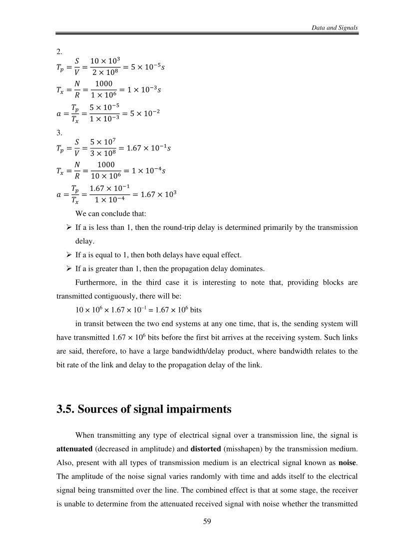
Data and Signals
59
2.
�� = � = 10 × 10,2 × 10% = 5 × 10'/)
�� = *+ = 10001 × 10. = 1 × 10',)
� = ���� = 5 × 10'/1 × 10', = 5 × 10'0
3.
�� = � = 5 × 10(3 × 10% = 1.67 × 10'4)
�� = *+ = 100010 × 10. = 1 × 10'5)
� = ���� = 1.67 × 10'41 × 10'5 = 1.67 × 10,
We can conclude that:
If a is less than 1, then the round-trip delay is determined primarily by the transmission
delay.
If a is equal to 1, then both delays have equal effect.
If a is greater than 1, then the propagation delay dominates.
Furthermore, in the third case it is interesting to note that, providing blocks are
transmitted contiguously, there will be:
10 × 106 × 1.67 × 10–1 = 1.67 × 106 bits
in transit between the two end systems at any one time, that is, the sending system will
have transmitted 1.67 × 106 bits before the first bit arrives at the receiving system. Such links
are said, therefore, to have a large bandwidth/delay product, where bandwidth relates to the
bit rate of the link and delay to the propagation delay of the link.
3.5. Sources of signal impairments
When transmitting any type of electrical signal over a transmission line, the signal is
attenuated (decreased in amplitude) and distorted (misshapen) by the transmission medium.
Also, present with all types of transmission medium is an electrical signal known as noise.
The amplitude of the noise signal varies randomly with time and adds itself to the electrical
signal being transmitted over the line. The combined effect is that at some stage, the receiver
is unable to determine from the attenuated received signal with noise whether the transmitted
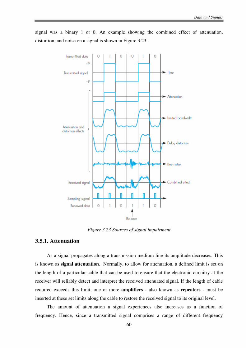
Data and Signals
60
signal was a binary 1 or 0. An example showing the combined effect of attenuation,
distortion, and noise on a signal is shown in Figure 3.23.
Figure 3.23 Sources of signal impairment
3.5.1. Attenuation
As a signal propagates along a transmission medium line its amplitude decreases. This
is known as signal attenuation. Normally, to allow for attenuation, a defined limit is set on
the length of a particular cable that can be used to ensure that the electronic circuitry at the
receiver will reliably detect and interpret the received attenuated signal. If the length of cable
required exceeds this limit, one or more amplifiers - also known as repeaters - must be
inserted at these set limits along the cable to restore the received signal to its original level.
The amount of attenuation a signal experiences also increases as a function of
frequency. Hence, since a transmitted signal comprises a range of different frequency

Data and Signals
61
components, this has the additional effect of distorting the received signal. To overcome this
problem, either the amplifiers are designed to amplify different frequency signals by varying
amounts or additional devices, known as equalizers, are used to equalize the amount of
attenuation across a defined band of frequencies.
The attenuation and amplification – also called gain – are measured in decibels (dB). If
the power level of the transmitted signaled is labeled P1 and the power of the received signal
is P2 then
67789:�7;<9 = 10 log4@ A4A0 BC
and
6DEF;G;H�7;<9 = 10 log4@ A0A4 BC
Since both P1 and P2 have the same unit of watts then decibels are dimensionless and
simply a measure of the relative magnitude of the two power levels. The use of logarithm
means that the overall attenuation/amplification of a multi-section transmission channel can
be determined simply by summing together the attenuation/amplification of the individual
sections.
Example
A transmission channel between two communicating equipment is made up of three
stations. The first introduces an attenuation of 16 dB, the second an amplification of 20 dB
and the third an attenuation of 10 dB. Assuming a mean transmitted power level of 400 mW,
determine the mean output power level of the channel
Solution 1
For first section: 16 = 10 log4@ 5@@IJ , hence P2 ≈ 10.0475 mW
For second section: 20 = 10 log4@ IJ4@.@5(/, hence P2 = 1004.75 mW
For third section: 10 = 10 log4@ 4@@5.(/IJ , hence P2 = 100.475 mW
That is, the mean output power level is 100.475 mW.
Solution 2
Overall attenuation of channel is 16 – 20 + 10 = 6dB
Hence 6 = 10 log4@ 5@@IJ and P2 = 100.475 mW
Data and Signals
62
3.5.2. Delay distortion
The rate of propagation of a sinusoidal signal along a transmission line varies with the
frequency of the signal. Consequently, when transmitting a digital signal the various
frequency components making up the signal arrive at the receiver with varying delays
between them. The effect of this is that the received signal is distorted and this is known as
delay distortion. The amount of distortion increases as the bit rate of the transmitted data
increases for the following reason: as the bit rate increases, so some of the frequency
components associated with each bit transition are delayed and start to interfere with the
frequency components associated with a later bit. Delay distortion is also known therefore as
inter-symbol interference and its effect is to vary the bit transition instants of the received
signal. Consequently, since the received signal is normally sampled at the nominal center of
each bit cell, this can lead to incorrect interpretation of the received signal as the bit rate
increases.
3.5.3. Noise
For any data transmission event, the received signal will consist of the transmitted
signal, modified by the various distortions imposed by the transmission system, plus
additional unwanted signals that are inserted somewhere between transmission and reception.
The latter, undesired signals are referred to as noise. Noise is the major limiting factor in
communications system performance.
While it can be defined in Watts, the noise is also usually expressed in a new unit called
decibel-Watt (dBW). The decibel-Watt is the strength of a signal expressed in decibels
relative to one Watt:
A<K8L�MN = 10 log4@ AN1 O BCO
where
PowerdBW = the power in decibel-Watt
PW = the power in watts
Another common unit is the dBm (decibel-milliWatt), which uses 1 mW as the
reference. The formula is:
A<K8L�M� = 10 log4@ A�N1 DO BCD
Note the following relationships:

Data and Signals
63
0 dBm = -30 dBW
+30 dBm = 0 dBW
Noise may be divided into four categories:
Thermal noise
Intermodulation noise
Crosstalk
Impulse noise
Thermal noise is due to thermal agitation of electrons. It is present in all electronic
devices and transmission media and is a function of temperature. Thermal noise is uniformly
distributed across the bandwidths typically used in communications systems and hence is
often referred to as white noise. Thermal noise cannot be eliminated and therefore places an
upper bound on communications system performance. Because of the weakness of the signal
received by satellite earth stations, thermal noise is particularly significant for satellite
communication.
The amount of thermal noise to be found in a bandwidth of 1 Hz in any device or
conductor is
*@ = P�
where
N0 = noise power density in watts per 1 Hz of bandwidth
k = Boltzmann’s constant = 1.38 * 10-23 J/K
T = temperature, in Kelvins
The noise is assumed to be independent of frequency. Thus the thermal noise in watts
present in a bandwidth of B Hertz can be expressed as * = P� C
The thermal noise can be expressed in decibel-Watt using the following equation:
* = 10 log4@ P�C = log4@ P + log4@ � + log4@ C = −228.6BCO + log4@ � + log4@ C
Example
Given a receiver with an effective noise temperature of 21°C and a 10-MHz bandwidth,
compute the thermal noise level at the receiver’s output, in dBW:
Solution
T = 21 + 273 = 294K
B = 10*106 = 107Hz

Data and Signals
64
N0 = -228.6 + 10 log10(294) + 10 log10(107)
= -228.6 + 24.7 + 70
= -133.9 dBW
When signals at different frequencies share the same transmission medium, the result
may be intermodulation noise. The effect of intermodulation noise is to produce signals at a
frequency that is the sum or difference of the two original frequencies or multiples of those
frequencies. For example, the mixing of signals at frequencies f1 and f2 might produce energy
at the frequency f1 + f2.This derived signal could interfere with an intended signal at the
frequency f1 + f2.
Intermodulation noise is produced by nonlinearities in the transmitter, receiver, and/or
intervening transmission medium. Ideally, these components behave as linear systems; that is,
the output is equal to the input times a constant. However, in any real system, the output is a
more complex function of the input. Excessive nonlinearity can be caused by component
malfunction or overload from excessive signal strength. It is under these circumstances that
the sum and difference frequency terms occur.
Crosstalk has been experienced by anyone who, while using the telephone, has been
able to hear another conversation; it is an unwanted coupling between signal paths. It can
occur by electrical coupling between nearby twisted pairs or, rarely, coax cable lines carrying
multiple signals. Crosstalk can also occur when microwave antennas pick up unwanted
signals; although highly directional antennas are used, microwave energy does spread during
propagation. Typically, crosstalk is of the same order of magnitude as, or less than, thermal
noise.
There are several types of crosstalk but in most cases the most limiting impairment is
near-end crosstalk or NEXT. This is also known as self-crosstalk since it is caused by the
strong signal output by a transmitter circuit being coupled (and hence interfering) with the
much weaker signal at the input to the local receiver circuit. As it can be observed in Figure
3.23, the received signal is normally significantly attenuated and distorted and hence the
amplitude of the coupled signal from the transmit section can be comparable with the
amplitude of the received signal.
Special integrated circuits known as adaptive NEXT cancelers are now used to
overcome this type of impairment. A typical arrangement is shown in Figure 3.24. The
canceler circuit adaptively forms an attenuated replica of the crosstalk signal that is coupled
into the receive line from the local transmitter and this is subtracted from the received signal.
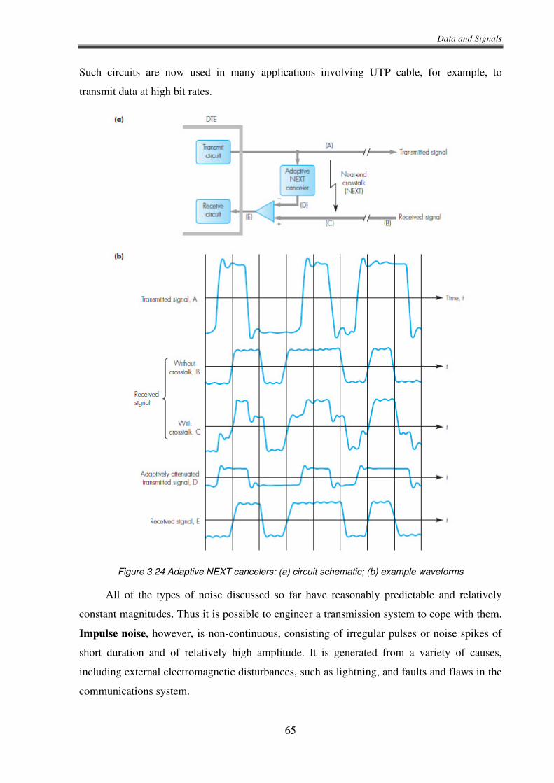
Data and Signals
65
Such circuits are now used in many applications involving UTP cable, for example, to
transmit data at high bit rates.
Figure 3.24 Adaptive NEXT cancelers: (a) circuit schematic; (b) example waveforms
All of the types of noise discussed so far have reasonably predictable and relatively
constant magnitudes. Thus it is possible to engineer a transmission system to cope with them.
Impulse noise, however, is non-continuous, consisting of irregular pulses or noise spikes of
short duration and of relatively high amplitude. It is generated from a variety of causes,
including external electromagnetic disturbances, such as lightning, and faults and flaws in the
communications system.

Data and Signals
66
Impulse noise is generally only a minor annoyance for analog data. For example, voice
transmission may be corrupted by short clicks and crackles with no loss of intelligibility.
However, impulse noise is the primary source of error in digital data communication. For
example, a sharp spike of energy of 0.01 s duration would not destroy any voice data but
would wash out about 560 bits of digital data being transmitted at 56 kbps.
3.5.4. Limited bandwidth
Since a typical digital signal is comprised of a large number of different frequency
components, then only those frequency components that are within the bandwidth of the
transmission medium are received. Because the amplitude of each frequency component
making up a digital signal diminishes with increasing frequency, it can be concluded that the
larger the bandwidth of the medium, the more higher frequency components are passed and
hence a more faithful reproduction of the original (transmitted) signal is received.
3.6. Channel capacity
We have seen that there are a variety of impairments that distort or corrupt a signal. For
digital data, the question that then arises is to what extent these impairments limit the data rate
that can be achieved. The maximum rate at which data can be transmitted over a given
communication path, or channel, under given conditions, is referred to as the channel
capacity.
There are four concepts here that we are trying to relate to one another.
Data rate: The rate, in bits per second (bps), at which data can be communicated
Bandwidth: The bandwidth of the transmitted signal as constrained by the transmitter
and the nature of the transmission medium, expressed in cycles per second, or Hertz
Noise: The average level of noise over the communications path
Error rate: The rate at which errors occur, where an error is the reception of a 1 when a
0 was transmitted or the reception of a 0 when a 1 was transmitted
The problem we are addressing is this: Communications facilities are expensive and, in
general, the greater the bandwidth of a facility, the greater the cost. Furthermore, all
transmission channels of any practical interest are of limited bandwidth. The limitations arise
from the physical properties of the transmission medium or from deliberate limitations at the
Data and Signals
67
transmitter on the bandwidth to prevent interference from other sources. Accordingly, we
would like to make as efficient use as possible of a given bandwidth. For digital data, this
means that we would like to get a data rate as high as possible at a particular limit of error rate
for a given bandwidth. The main constraint on achieving this efficiency is noise.
3.6.1. Nyquist Bandwidth
To begin, let us consider the case of a channel that is noise free. In this environment, the
limitation on data rate is simply the bandwidth of the signal. A formulation of this limitation,
due to Nyquist, states that if the rate of signal transmission is 2B, then a signal with
frequencies no greater than B is sufficient to carry the signal rate. The converse is also true:
Given a bandwidth of B, the highest signal rate that can be carried is 2B. This limitation is
due to the effect of inter-symbol interference, such as is produced by delay distortion.
If the signals to be transmitted are binary (two voltage levels), then the data rate that can
be supported by B Hz is 2B bps. However, signals with more than two levels, that is, each
signal element can represent more than one bit, are often used in data communication. For
example, if four possible voltage levels are used as signals, then each signal element can
represent two bits. With multilevel signaling, the Nyquist formulation becomes T = 2C log0 U
where M is the number of discrete signal or voltage levels. The previous formula is also
known as Hartley’s law.
So, for a given bandwidth, the data rate can be increased by increasing the number of
different signal elements. However, this places an increased burden on the receiver: Instead of
distinguishing one of two possible signal elements during each signal time, it must distinguish
one of M possible signal elements. Noise and other impairments on the transmission line will
limit the practical value of M.
Example
A modem to be used with a PSTN uses a modulation scheme with eight levels per
signaling element. If the bandwidth of the PSTN is 3100 Hz, deduce the Nyquist maximum
data transfer rate.
Solution
C = 2Blog2M
= 2 x 3100 x log28

Data and Signals
68
= 2 x 3100 x 3
= 18 600 bps
3.6.2. Shannon Capacity Formula
Nyquist’s formula indicates that, all other things being equal, doubling the bandwidth
doubles the data rate. Now consider the relationship among data rate, noise, and error rate.
The presence of noise can corrupt one or more bits. If the data rate is increased, then the bits
become “shorter” so that more bits are affected by a given pattern of noise.
All of these concepts can be tied together neatly in a formula developed by the
mathematician Claude Shannon. As we have just illustrated, the higher the data rate, the more
damage that unwanted noise can do. For a given level of noise, we would expect that a greater
signal strength would improve the ability to receive data correctly in the presence of noise.
The key parameter involved in this reasoning is the signal-to-noise ratio (SNR, or S/N),
which is the ratio of the power in a signal to the power contained in the noise that is present at
a particular point in the transmission. Typically, this ratio is measured at a receiver, because it
is at this point that an attempt is made to process the signal and recover the data.
�*+ = );V9�F E<K8L9<;)8 E<K8L For convenience, this ratio is often reported in decibels: �*+�M = 10 log4@ �*+
This expresses the amount, in decibels, that the intended signal exceeds the noise level.
A high SNR will mean a high-quality signal and a low number of required intermediate
repeaters.
The signal-to-noise ratio is important in the transmission of digital data because it sets
the upper bound on the achievable data rate. Shannon’s result (also known as Shannon-
Hartley law) is that the maximum channel capacity, in bits per second, obeys the equation
T = C log0(1 + �*+)
where C is the capacity of the channel in bits per second and B is the bandwidth of the
channel in Hertz. The Shannon formula represents the theoretical maximum that can be
achieved. In practice, however, only much lower rates are achieved. One reason for this is that
the formula assumes white noise (thermal noise). Impulse noise is not accounted for, nor are
attenuation distortion or delay distortion. Even in an ideal white noise environment, present
technology still cannot achieve Shannon capacity due to encoding issues, such as coding
length and complexity.

Data and Signals
69
The capacity indicated in the preceding equation is referred to as the error-free capacity.
Shannon proved that if the actual information rate on a channel is less than the error-free
capacity, then it is theoretically possible to use a suitable signal code to achieve error-free
transmission through the channel. Shannon’s theorem unfortunately does not suggest a means
for finding such codes, but it does provide a yardstick by which the performance of practical
communication schemes may be measured.
Several other observations concerning the preceding equation may be instructive. For a
given level of noise, it would appear that the data rate could be increased by increasing either
signal strength or bandwidth. However, as the signal strength increases, so do the effects of
nonlinearities in the system, leading to an increase in intermodulation noise. Note also that,
because noise is assumed to be white, the wider the bandwidth, the more noise is admitted to
the system. Thus, as B increases, SNR decreases.
Example
Assuming that a PSTN has a bandwidth of 3000 Hz and a typical signal-to-noise ratio of
20 dB, determine the maximum theoretical information (data) rate that can be obtained.
Solution
Because: �*+�M = 10 log4@ �*+
It results that: 20 = 10 log4@ �*+
Therefore:
SNR = 100
Now:
T = C log0(1 + �*+)
Therefore: T = 3000 log0(1 + 100) ≈ 19963 [E)
3.6.3. The expression Eb / N0
Another parameter related to SNR that is more convenient for determining digital data
rates and error rates and that is the standard quality measure for digital communication system
performance. The parameter is the ratio of signal energy per bit to noise power density per
Hertz, Eb/N0. Consider a signal, digital or analog, that contains binary digital data transmitted
Data and Signals
70
at a certain bit rate R. Recalling that 1Watt = 1 J/s, the energy per bit in a signal is given by \� = ��� where S is the signal power and Tb is the time required to send one bit. The data
rate R is just R = 1/Tb .Thus \�*@ = � +⁄*@ = �P�+
or, in decibel notation,
^\�*@_�� = 10 log4@ ^\�*@_ = 10 log4@ ^ �P�+_= ��MN − 10 log4@ P − 10 log4@ � − 10 log4@ += ��MN + 228.6 B[O − 10 log4@ � − 10 log4@ +
The ratio Eb/N0 is important because the bit error rate for digital data is a (decreasing)
function of this ratio. Given a value of needed to achieve a desired error rate, the parameters
in the preceding formula may be selected. Note that as the bit rate R increases, the transmitted
signal power, relative to noise, must increase to maintain the required Eb/N0.
The advantage of over SNR is that the latter quantity depends on the bandwidth. We can
relate Eb/N0 to SNR as follows: \�*@ = �*@+
The parameter N0 is the noise power density in Watts/Hertz. Hence, the noise in a signal
with bandwidth B is N = N0B. Substituting, we have \�*@ = �* C+
Another formulation of interest relates Eb/N0 to spectral efficiency C/B. Shannon’s
result can be rewritten as:
�*+ = 2` M⁄ − 1
By combining the previous two equations and by equating R with C we obtain: \�*@ = CT a2` M⁄ − 1b
This is a useful formula that relates the achievable spectral efficiency C/B to Eb/N0.
Example
Compute the minimum Eb/N0 required to achieve a spectral efficiency of 6 bps/Hz.
Solution
Eb/N0 = (1/6)(26 – 1) = 10.5 ≈ 10.21 dB.
Data Transmission
71
4. Data Transmission
4.1. Data codes
All electronic digital equipment operate using a fixed number of binary digits to
represent a single element of data or word. Within a computer, for example, this may be 8,
16, 32 or 64 bits; data requiring more than this precision are represented by multiples of these
elements. Because of this range of bits to represent each word, it is usual when
communicating data between two pieces of equipment to use multiple fixed-length elements,
each of 8 bits. In some applications the 8 bits may represent a binary encoded alphabetic or
numeric (alphanumeric) character while in others it may represent an 8-bit component of a
larger value. In the latter case, the component is often referred to as an 8-bit byte; but, in
general, within the communication facility, each 8-bit element is simply referred to as an
octet.
One of the most common forms of data transmitted between a transmitter and a receiver
is textual data. For example, banking institutions that wish to transfer money often transmit
textual information, such as account numbers, names of account owners, bank names,
addresses, and the amount of money to be transferred. This textual information is transmitted
as a sequence of characters. To distinguish one character from another, each character is
represented by a unique binary pattern of 1s and 0s. The set of all textual characters or
symbols and their corresponding binary patterns is called a data code. Two important data
codes are ASCII, and Unicode.
4.1.1. ASCII
The American Standard Code for Information Interchange (ASCII) is a government
standard in the United States and is one of the most widely used data codes in the world. The
ASCII character set uses 7 bits that allows for 128 (27 = 128) possible combinations of textual
symbols, representing uppercase and lowercase letters, the digits 0 to 9, special symbols, and
control characters. Because the byte, which consists of 8 bits, is a common unit of data, the 7-
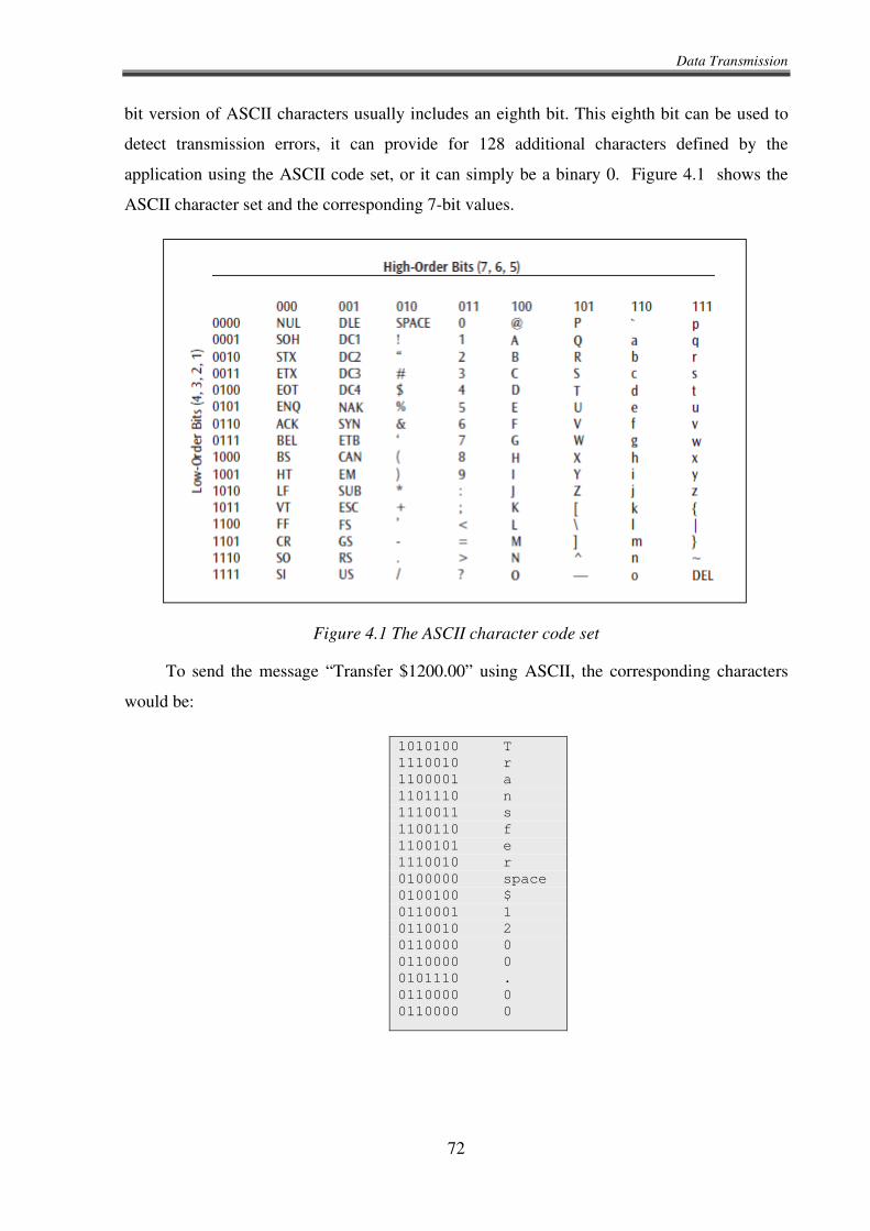
Data Transmission
72
bit version of ASCII characters usually includes an eighth bit. This eighth bit can be used to
detect transmission errors, it can provide for 128 additional characters defined by the
application using the ASCII code set, or it can simply be a binary 0. Figure 4.1 shows the
ASCII character set and the corresponding 7-bit values.
Figure 4.1 The ASCII character code set
To send the message “Transfer $1200.00” using ASCII, the corresponding characters
would be:
1010100 T
1110010 r
1100001 a
1101110 n
1110011 s
1100110 f
1100101 e
1110010 r
0100000 space
0100100 $
0110001 1
0110010 2
0110000 0
0110000 0
0101110 .
0110000 0
0110000 0
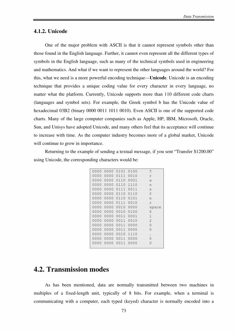
Data Transmission
73
4.1.2. Unicode
One of the major problem with ASCII is that it cannot represent symbols other than
those found in the English language. Further, it cannot even represent all the different types of
symbols in the English language, such as many of the technical symbols used in engineering
and mathematics. And what if we want to represent the other languages around the world? For
this, what we need is a more powerful encoding technique—Unicode. Unicode is an encoding
technique that provides a unique coding value for every character in every language, no
matter what the platform. Currently, Unicode supports more than 110 different code charts
(languages and symbol sets). For example, the Greek symbol b has the Unicode value of
hexadecimal 03B2 (binary 0000 0011 1011 0010). Even ASCII is one of the supported code
charts. Many of the large computer companies such as Apple, HP, IBM, Microsoft, Oracle,
Sun, and Unisys have adopted Unicode, and many others feel that its acceptance will continue
to increase with time. As the computer industry becomes more of a global market, Unicode
will continue to grow in importance.
Returning to the example of sending a textual message, if you sent “Transfer $1200.00”
using Unicode, the corresponding characters would be:
4.2. Transmission modes
As has been mentioned, data are normally transmitted between two machines in
multiples of a fixed-length unit, typically of 8 bits. For example, when a terminal is
communicating with a computer, each typed (keyed) character is normally encoded into a
0000 0000 0101 0100 T
0000 0000 0111 0010 r
0000 0000 0110 0001 a
0000 0000 0110 1110 n
0000 0000 0111 0011 s
0000 0000 0110 0110 f
0000 0000 0110 0101 e
0000 0000 0111 0010 r
0000 0000 0010 0000 space
0000 0000 0010 0100 $
0000 0000 0011 0001 1
0000 0000 0011 0010 2
0000 0000 0011 0000 0
0000 0000 0011 0000 0
0000 0000 0010 1110 .
0000 0000 0011 0000 0
0000 0000 0011 0000 0
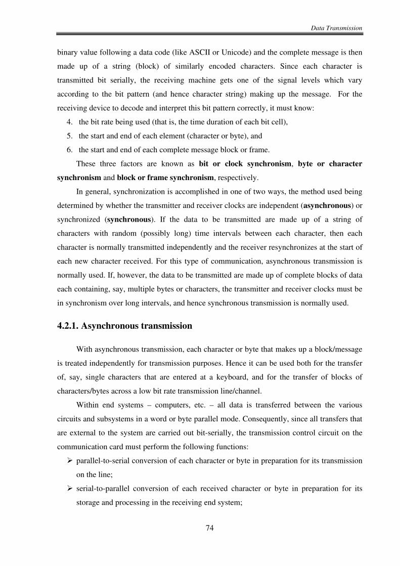
Data Transmission
74
binary value following a data code (like ASCII or Unicode) and the complete message is then
made up of a string (block) of similarly encoded characters. Since each character is
transmitted bit serially, the receiving machine gets one of the signal levels which vary
according to the bit pattern (and hence character string) making up the message. For the
receiving device to decode and interpret this bit pattern correctly, it must know:
4. the bit rate being used (that is, the time duration of each bit cell),
5. the start and end of each element (character or byte), and
6. the start and end of each complete message block or frame.
These three factors are known as bit or clock synchronism, byte or character
synchronism and block or frame synchronism, respectively.
In general, synchronization is accomplished in one of two ways, the method used being
determined by whether the transmitter and receiver clocks are independent (asynchronous) or
synchronized (synchronous). If the data to be transmitted are made up of a string of
characters with random (possibly long) time intervals between each character, then each
character is normally transmitted independently and the receiver resynchronizes at the start of
each new character received. For this type of communication, asynchronous transmission is
normally used. If, however, the data to be transmitted are made up of complete blocks of data
each containing, say, multiple bytes or characters, the transmitter and receiver clocks must be
in synchronism over long intervals, and hence synchronous transmission is normally used.
4.2.1. Asynchronous transmission
With asynchronous transmission, each character or byte that makes up a block/message
is treated independently for transmission purposes. Hence it can be used both for the transfer
of, say, single characters that are entered at a keyboard, and for the transfer of blocks of
characters/bytes across a low bit rate transmission line/channel.
Within end systems – computers, etc. – all data is transferred between the various
circuits and subsystems in a word or byte parallel mode. Consequently, since all transfers that
are external to the system are carried out bit-serially, the transmission control circuit on the
communication card must perform the following functions:
parallel-to-serial conversion of each character or byte in preparation for its transmission
on the line;
serial-to-parallel conversion of each received character or byte in preparation for its
storage and processing in the receiving end system;

Data Transmission
75
a means for the receiver to achieve bit, character, and frame synchronization;
the generation of suitable error check digits for error detection and the detection of such
errors at the receiver should they occur.
Figure 4.2 Asynchronous transmission: (a) principle of operation; (b) timing principles
As it can be observer in Figure 4.2 (a), parallel-to-serial conversion is performed by a
parallel-in, serial-out (PISO) shift register. This, as its name implies, allows a complete
character or byte to be loaded in parallel and then shifted out bit-serially. Similarly, serial-to-
parallel conversion is performed by a serial-in, parallel- out (SIPO) shift register, which
executes the reverse function.

Data Transmission
76
To achieve bit and character synchronization, we must set the receiving transmission
control circuit (which is normally programmable) to operate with the same characteristics as
the transmitter in terms of the number of bits per character and the bit rate being used.
Bit synchronization
In asynchronous transmission, the receiver clock (which is used to sample and shift the
incoming signal into the SIPO shift register) runs asynchronously with respect to the
incoming signal. In order for the reception process to work reliably, we must devise a scheme
whereby the local (asynchronous) receiver clock samples (and hence shifts into the SIPO shift
register) the incoming signal as near to the center of the bit cell as possible.
To achieve this, each character/byte to be transmitted is encapsulated between a start bit
and one or two stop bits. As it is presented in Figure 4.2 (a), the start bit is a binary 0 (and
known as a space) and the stop bit a binary 1 (and known as a mark). When transmitting a
block comprising a string of characters/bytes, the start bit of each character/byte immediately
follows the stop bit(s) of the previous character/byte. When transmitting random characters,
however, the line stays at the stop/1 level until the next character is to be transmitted. Hence
between blocks (or after each character), the line is said to be marking (time).
The use of a start and stop bit per character/byte of different polarities means that,
irrespective of the binary contents of each character/byte, there is a guaranteed 1→0 transition
at the start of each new character/byte. A local receiver clock of N times the transmitted bit
rate (N= 16 is common) is used and each new bit is shifted into the SIPO shift register after N
cycles of this clock. The first 1→0 transition associated with the start bit of each character is
used to start the counting process. Each bit (including the start bit) is sampled at
(approximately) the center of each bit cell. After the first transition is detected, the signal (the
start bit) is sampled after N/2 clock cycles and then subsequently after N clock cycles for each
bit in the character and also the stop bit(s). Three examples of different clock rate ratios are
shown in Figure 4.3.
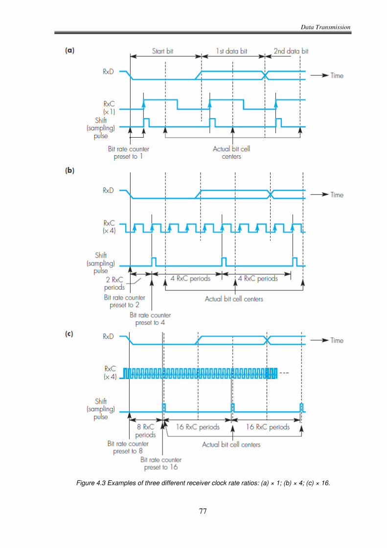
Data Transmission
77
Figure 4.3 Examples of three different receiver clock rate ratios: (a) × 1; (b) × 4; (c) × 16.
Data Transmission
78
Remembering that the receiver clock (RxC) is running asynchronously with respect to
the incoming signal (RxD), the relative positions of the two signals can be anywhere within a
single cycle of the receiver clock. Those shown in the figure are just arbitrary positions.
Nevertheless, we can deduce from these examples that the higher the clock rate ratio, the
nearer the sampling instant will be to the nominal bit cell center. Because of this mode of
operation, the maximum bit rate normally used with asynchronous transmission is 19.2 kbps.
Example
A block of data is to be transmitted across a serial data link. If a clock of 19.2 kHz is
available at the receiver, deduce the suitable clock rate ratios and estimate the worst-case
deviations from the nominal bit cell centers, expressed as a percentage of a bit period, for
each of the following data transmission rates:
7. 1200bps
8. 2400bps
9. 9600bps
Solution
It can readily be deduced from Figure 4.3 that the worst-case deviation from the
nominal bit cell centers is approximately plus or minus one half of one cycle of the receiver
clock.
Hence:
10. At 1200 bps, the maximum RxC ratio can be × 16. The maximum deviation is thus ±
3.125%.
11. At 2400 bps, the maximum RxC ratio can be × 8. The maximum deviation is thus ±
6.25%.
12. At 9600 bps, the maximum RxC ratio can be × 2. The maximum deviation is thus ±
25%.
Character synchronization
As indicated above, the receiving transmission control circuit is programmed to operate
with the same number of bits per character and the same number of stop bits as the
transmitter. After the start bit has been detected and received, the receiver achieves character
synchronization simply by counting the programmed number of bits. It then transfers the
received character/byte into a local buffer register and signals to the controlling device (a
microprocessor, for example) on the communication card that a new character/byte has been
Data Transmission
79
received. It then awaits the next line signal transition that indicates a new start bit (and hence
character) is being received.
Frame synchronization
When messages comprising blocks of characters or bytes – normally referred to as
information frames – are being transmitted, in addition to bit and character synchronization,
the receiver must be able to determine the start and end of each frame. This is known as
frame synchronization.
The simplest method of transmitting blocks of printable characters is to encapsulate the
complete block between two special (nonprintable) transmission control characters: STX
(start-of-text), which indicates the start of a new frame after an idle period, and ETX (end-of-
text), which indicates the end of the frame. As the frame contents consist only of printable
characters, the receiver can interpret the receipt of an STX character as signaling the start of a
new frame and an ETX character as signaling the end of the frame. This is shown in Figure
4.4(a).
Although the scheme shown is satisfactory for the transmission of blocks of printable
characters, when transmitting blocks that comprise strings of bytes (for example, the contents
of a file containing compressed speech or video), the use of a single ETX character to indicate
the end of a frame is not sufficient. In the case of a string of bytes, one of the bytes might be
the same as an ETX character, which would cause the receiver to terminate the reception
process abnormally.
To overcome this problem, when transmitting this type of data the two transmission
control characters STX and ETX are each preceded by a third transmission control character
known as data link escape (DLE). The modified format of a frame is then as shown in Figure
4.4 (b).
Remember that the transmitter knows the number of bytes in each frame to be
transmitted. After transmitting the start-of-frame sequence (DLE-STX), the transmitter
inspects each byte in the frame prior to transmission to determine if it is the same as the DLE
character pattern. If it is, irrespective of the next byte, a second DLE character (byte) is
transmitted before the next byte. This procedure is repeated until the appropriate number of
bytes in the frame have been transmitted. The transmitter then signals the end of the frame by
transmitting the unique DLE-STX sequence.
This procedure is known as character or byte stuffing. On receipt of each byte after
the DLE-STX start-of-frame sequence, the receiver determines whether it is a DLE character
Data Transmission
80
(byte). If it is, the receiver then processes the next byte to determine whether that is another
DLE or an ETX. If it is a DLE, the receiver discards it and awaits the next byte. If it is an
ETX, this can reliably be taken as being the end of the frame.
Figure 4.4 Frame synchronization with different frame contents: (a) printable characters; (b) string of bytes.
4.2.2. Synchronous transmission
The use of an additional start bit and one or more stop bits per character or byte means
that asynchronous transmission is relatively inefficient in its use of transmission capacity,
especially when transmitting messages that comprise large blocks of characters or bytes. Also,
the bit (clock) synchronization method used with asynchronous transmission becomes less
reliable as the bit rate increases. This results, firstly, from the fact that the detection of the first
Data Transmission
81
start bit transition is only approximate and, secondly, although the receiver clock operates at
N times the nominal transmit clock rate, because of tolerances there are small differences
between the two that can cause the sampling instant to drift during the reception of a character
or byte. The synchronous transmission is normally used to overcome these problems. As with
asynchronous transmission, however, a suitable method to enable the receiver to achieve bit
(clock) character (byte) and frame (block) synchronization must be selected. In practice, there
are two synchronous transmission control schemes: character-oriented and bit-oriented. Each
will be discussed separately but, since they both use the same bit synchronization methods,
those methods will be discussed first.
Bit synchronization
Although the presence of a start bit and stop bit(s) with each character is often used to
discriminate between asynchronous and synchronization transmission, the fundamental
difference between the two methods is that with asynchronous transmission the receiver clock
runs asynchronously (unsynchronized) with respect to the incoming (received) signal,
whereas with synchronous transmission the receiver clock operates in synchronism with the
received signal.
As it was already indicated, start and stop bits are not used with synchronous
transmission. Instead each frame is transmitted as a continuous stream of binary digits. The
receiver then obtains (and maintains) bit synchronization in one of two ways. Either the clock
(timing) information is embedded into the transmitted signal and subsequently extracted by
the receiver, or the receiver has a local clock (as with asynchronous transmission) but this
time it is kept in synchronism with the received signal by a device known as a digital phase-
lock-loop (DPLL). As it will be soon presented, the DPLL exploits the 1→0 or 0→1 bit
transitions in the received signal to maintain bit (clock) synchronism over an acceptably long
period. Hybrid schemes that exploit both methods are also used. The principles of operation
of both schemes are shown in Figure 4.5.
Clock encoding and extraction The alternative methods of embedding timing (clock)
information into a transmitted bit-stream are shown in Figure 4.6. The scheme shown in part
(a) is the Manchester encoding and that in part (b) is the differential Manchester encoding.
As it was presented in the previous chapter, with Manchester encoding each bit is
encoded as either a low-high signal (binary 1) or a high-low signal (binary 0), both occupying
a single bit-cell period. Also, there is always a transition (high-low or low-high) at the center
of each bit cell. It is this that is used by the clock extraction circuit to produce a clock pulse
Data Transmission
82
that is then delayed to the center of the second half of the bit cell. At this point the received
(encoded) signal is either high (for binary 1) or low (for binary 0) and hence the correct bit is
sampled and shifted into the SIPO shift register.
Figure 4.5 Alternative bit/clock synchronization methods with synchronous transmission: (a) clock encoding; (b) digital phase-lock-loop (DPLL).
Figure 4.6 Synchronous transmission clock encoding examples: (a) Manchester; (b) differential Manchester
Data Transmission
83
The scheme shown in Figure 4.6(b) is differential Manchester encoding. As it was
already presented in the previous chapter, it differs from Manchester encoding in that
although there is still a transition at the center of each bit cell, a transition at the start of the bit
cell occurs only if the next bit to be encoded is a 0. This has the effect that the encoded output
signal may take on one of two forms depending on the assumed start level (high or low). As
we can see, however, one is simply an inverted version of the other and this is the origin of
the term “differential”. The extracted clock is generated at the start of each bit cell. At this
point the received (encoded) signal either changes – for example, from +2V to –2V or from
-2V to +2V in which case a binary 0 is shifted into the SIPO – or remains at the same level, in
which case a binary 1 is shifted into the SIPO.
The two Manchester encoding schemes are balanced codes which means there is no
mean (DC) value associated with them. This is so since a string of binary 1s (or 0s) will
always have transitions associated with them rather than a constant (DC) level. This is an
important feature since it means that the received signal can be AC coupled to the receiver
electronics using a transformer. The receiver electronics can then operate using its own power
supply since this is effectively isolated from the power supply of the transmitter.
Digital phase-lock-loop An alternative approach to encoding the clock in the
transmitted bit stream is to utilize a stable clock source at the receiver which is kept in time
synchronism with the incoming bit stream. However, as there are no start and stop bits with a
synchronous transmission scheme, the information must be encoded in such a way that there
are always sufficient bit transitions (1→0 or 0→1) in the transmitted waveform to enable the
receiver clock to be resynchronized at frequent intervals. One approach is to pass the data to
be transmitted through a scrambler, which randomizes the transmitted bitstream so removing
contiguous strings of 1s or 0s. Alternatively, the data may be encoded in such a way that
suitable transitions will always be present.
The bit pattern to be transmitted is first differentially encoded, as it was presented in the
previous chapter, in Figure 3.10(b). With NRZI encoding the signal level (1 or 0) does not
change for the transmission of a binary 0, whereas a binary 1 causes a change. This means
that there will always be bit transitions in the incoming signal of an NRZI waveform,
providing there are no contiguous streams of binary 0s. This can be obtained by using, for
example, a 4B5B encoding scheme. Consequently, the resulting waveform will contain a
guaranteed number of transitions, since long strings of 1s cause a transition every bit cell.
This enables the receiver to adjust its clock so that it is in synchronism with the incoming
bitstream.

Data Transmission
84
The circuit used to maintain bit synchronism is known as a digital phase-lock-loop
(DPLL) and is shown in Figure 4.7. A crystal-controlled oscillator (clock source), which can
hold its frequency sufficiently constant to require only very small adjustments at irregular
intervals, is connected to the DPLL.
Figure 4.7 DPLL circuit schematic
Typically, the frequency of the clock is 32 times the bit rate used on the data link and is
used by the DPLL to derive the timing interval between successive samples of the received
bitstream.
Assuming the incoming bitstream and the local clock are in synchronism, the state (1 or
0) of the incoming signal on the line will be sampled (and hence clocked into the SIPO shift
register) at the center of each bit cell with exactly 32 clock periods between each sample. This
is shown in Figure 4.8.
Figure 4.8 DPLL in phase operation
Now assume that the incoming bitstream and local clock drift out of synchronism
because of small variations in the latter. The sampling instant is adjusted in discrete
increments as shown in Figure 4.9. If there are no transitions on the line, the DPLL simply
generates a sampling pulse every 32 clock periods after the previous one. Whenever a
transition (1→0 or 0→1) is detected, the time interval between the previously generated
sampling pulse and the next is determined according to the position of the transition relative
to where the DPLL thought it should occur. To achieve this, each bit period is divided into
five segments, shown as A, B, C, D, and E in the figure. For example, a transition occurring
during segment A indicates that the last sampling pulse was too close to the next transition
and hence late. The time period to the next pulse is therefore shortened to 30 clock periods.
Similarly, a transition occurring in segment E indicates that the previous sampling pulse was
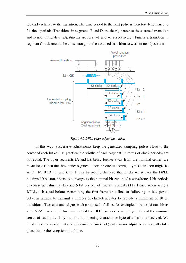
Data Transmission
85
too early relative to the transition. The time period to the next pulse is therefore lengthened to
34 clock periods. Transitions in segments B and D are clearly nearer to the assumed transition
and hence the relative adjustments are less (–1 and +1 respectively). Finally a transition in
segment C is deemed to be close enough to the assumed transition to warrant no adjustment.
Figure 4.9 DPLL clock adjustment rules
In this way, successive adjustments keep the generated sampling pulses close to the
center of each bit cell. In practice, the widths of each segment (in terms of clock periods) are
not equal. The outer segments (A and E), being further away from the nominal center, are
made longer than the three inner segments. For the circuit shown, a typical division might be
A=E= 10, B=D= 5, and C=2. It can be readily deduced that in the worst case the DPLL
requires 10 bit transitions to converge to the nominal bit center of a waveform: 5 bit periods
of coarse adjustments (±2) and 5 bit periods of fine adjustments (±1). Hence when using a
DPLL, it is usual before transmitting the first frame on a line, or following an idle period
between frames, to transmit a number of characters/bytes to provide a minimum of 10 bit
transitions. Two characters/bytes each composed of all 1s, for example, provide 16 transitions
with NRZI encoding. This ensures that the DPLL generates sampling pulses at the nominal
center of each bit cell by the time the opening character or byte of a frame is received. We
must stress, however, that once in synchronism (lock) only minor adjustments normally take
place during the reception of a frame.
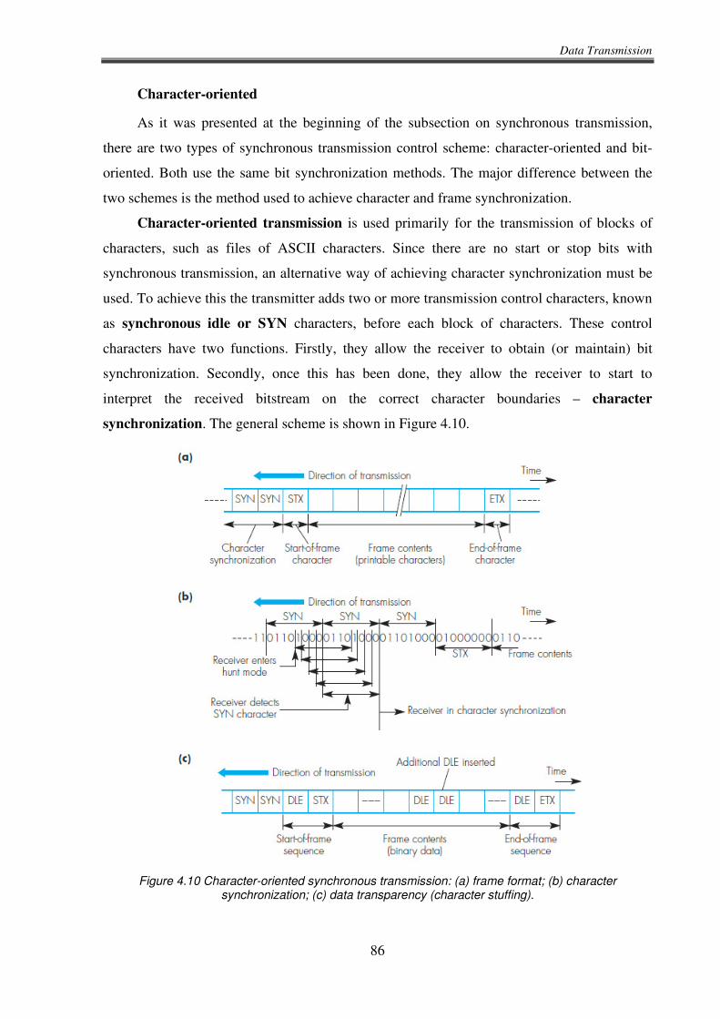
Data Transmission
86
Character-oriented
As it was presented at the beginning of the subsection on synchronous transmission,
there are two types of synchronous transmission control scheme: character-oriented and bit-
oriented. Both use the same bit synchronization methods. The major difference between the
two schemes is the method used to achieve character and frame synchronization.
Character-oriented transmission is used primarily for the transmission of blocks of
characters, such as files of ASCII characters. Since there are no start or stop bits with
synchronous transmission, an alternative way of achieving character synchronization must be
used. To achieve this the transmitter adds two or more transmission control characters, known
as synchronous idle or SYN characters, before each block of characters. These control
characters have two functions. Firstly, they allow the receiver to obtain (or maintain) bit
synchronization. Secondly, once this has been done, they allow the receiver to start to
interpret the received bitstream on the correct character boundaries – character
synchronization. The general scheme is shown in Figure 4.10.
Figure 4.10 Character-oriented synchronous transmission: (a) frame format; (b) character synchronization; (c) data transparency (character stuffing).
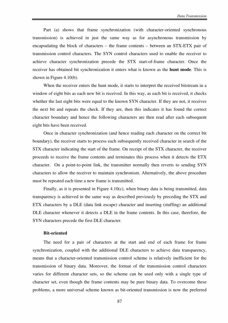
Data Transmission
87
Part (a) shows that frame synchronization (with character-oriented synchronous
transmission) is achieved in just the same way as for asynchronous transmission by
encapsulating the block of characters – the frame contents – between an STX-ETX pair of
transmission control characters. The SYN control characters used to enable the receiver to
achieve character synchronization precede the STX start-of-frame character. Once the
receiver has obtained bit synchronization it enters what is known as the hunt mode. This is
shown in Figure 4.10(b).
When the receiver enters the hunt mode, it starts to interpret the received bitstream in a
window of eight bits as each new bit is received. In this way, as each bit is received, it checks
whether the last eight bits were equal to the known SYN character. If they are not, it receives
the next bit and repeats the check. If they are, then this indicates it has found the correct
character boundary and hence the following characters are then read after each subsequent
eight bits have been received.
Once in character synchronization (and hence reading each character on the correct bit
boundary), the receiver starts to process each subsequently received character in search of the
STX character indicating the start of the frame. On receipt of the STX character, the receiver
proceeds to receive the frame contents and terminates this process when it detects the ETX
character. On a point-to-point link, the transmitter normally then reverts to sending SYN
characters to allow the receiver to maintain synchronism. Alternatively, the above procedure
must be repeated each time a new frame is transmitted.
Finally, as it is presented in Figure 4.10(c), when binary data is being transmitted, data
transparency is achieved in the same way as described previously by preceding the STX and
ETX characters by a DLE (data link escape) character and inserting (stuffing) an additional
DLE character whenever it detects a DLE in the frame contents. In this case, therefore, the
SYN characters precede the first DLE character.
Bit-oriented
The need for a pair of characters at the start and end of each frame for frame
synchronization, coupled with the additional DLE characters to achieve data transparency,
means that a character-oriented transmission control scheme is relatively inefficient for the
transmission of binary data. Moreover, the format of the transmission control characters
varies for different character sets, so the scheme can be used only with a single type of
character set, even though the frame contents may be pure binary data. To overcome these
problems, a more universal scheme known as bit-oriented transmission is now the preferred
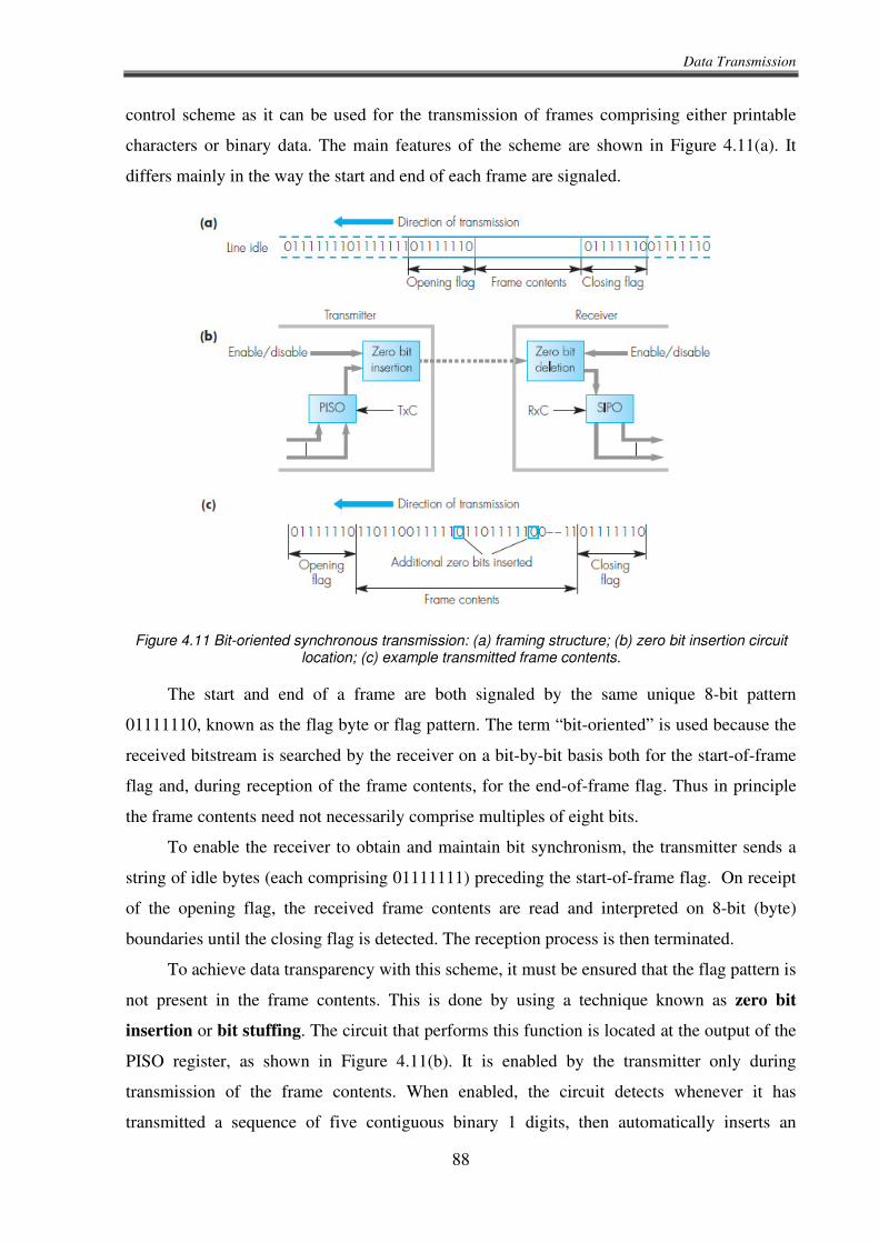
Data Transmission
88
control scheme as it can be used for the transmission of frames comprising either printable
characters or binary data. The main features of the scheme are shown in Figure 4.11(a). It
differs mainly in the way the start and end of each frame are signaled.
Figure 4.11 Bit-oriented synchronous transmission: (a) framing structure; (b) zero bit insertion circuit location; (c) example transmitted frame contents.
The start and end of a frame are both signaled by the same unique 8-bit pattern
01111110, known as the flag byte or flag pattern. The term “bit-oriented” is used because the
received bitstream is searched by the receiver on a bit-by-bit basis both for the start-of-frame
flag and, during reception of the frame contents, for the end-of-frame flag. Thus in principle
the frame contents need not necessarily comprise multiples of eight bits.
To enable the receiver to obtain and maintain bit synchronism, the transmitter sends a
string of idle bytes (each comprising 01111111) preceding the start-of-frame flag. On receipt
of the opening flag, the received frame contents are read and interpreted on 8-bit (byte)
boundaries until the closing flag is detected. The reception process is then terminated.
To achieve data transparency with this scheme, it must be ensured that the flag pattern is
not present in the frame contents. This is done by using a technique known as zero bit
insertion or bit stuffing. The circuit that performs this function is located at the output of the
PISO register, as shown in Figure 4.11(b). It is enabled by the transmitter only during
transmission of the frame contents. When enabled, the circuit detects whenever it has
transmitted a sequence of five contiguous binary 1 digits, then automatically inserts an

Data Transmission
89
additional binary 0 digit. In this way, the flag pattern 01111110 can never be present in the
frame contents between the opening and closing flags.
A similar circuit at the receiver located prior to the input of the SIPO shift receiver
performs the reverse function. Whenever a zero is detected after five contiguous 1 digits, the
circuit automatically removes (deletes) it from the frame contents. Normally the frame also
contains additional error detection digits preceding the closing flag which are subjected to the
same bit stuffing operation as the frame contents. An example stuffed bit pattern is shown in
Figure 4.11(c).
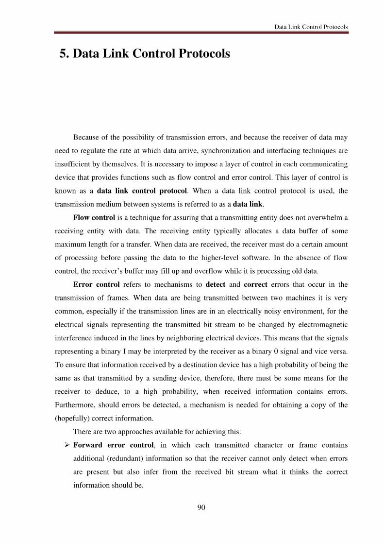
Data Link Control Protocols
90
5. Data Link Control Protocols
Because of the possibility of transmission errors, and because the receiver of data may
need to regulate the rate at which data arrive, synchronization and interfacing techniques are
insufficient by themselves. It is necessary to impose a layer of control in each communicating
device that provides functions such as flow control and error control. This layer of control is
known as a data link control protocol. When a data link control protocol is used, the
transmission medium between systems is referred to as a data link.
Flow control is a technique for assuring that a transmitting entity does not overwhelm a
receiving entity with data. The receiving entity typically allocates a data buffer of some
maximum length for a transfer. When data are received, the receiver must do a certain amount
of processing before passing the data to the higher-level software. In the absence of flow
control, the receiver’s buffer may fill up and overflow while it is processing old data.
Error control refers to mechanisms to detect and correct errors that occur in the
transmission of frames. When data are being transmitted between two machines it is very
common, especially if the transmission lines are in an electrically noisy environment, for the
electrical signals representing the transmitted bit stream to be changed by electromagnetic
interference induced in the lines by neighboring electrical devices. This means that the signals
representing a binary I may be interpreted by the receiver as a binary 0 signal and vice versa.
To ensure that information received by a destination device has a high probability of being the
same as that transmitted by a sending device, therefore, there must be some means for the
receiver to deduce, to a high probability, when received information contains errors.
Furthermore, should errors be detected, a mechanism is needed for obtaining a copy of the
(hopefully) correct information.
There are two approaches available for achieving this:
Forward error control, in which each transmitted character or frame contains
additional (redundant) information so that the receiver cannot only detect when errors
are present but also infer from the received bit stream what it thinks the correct
information should be.
Data Link Control Protocols
91
Feedback error control, in which each character or frame includes only sufficient
additional information to enable the receiver to detect when errors are present and then
to employ a retransmission scheme to request that another, hopefully correct, copy of
the erroneous information be sent.
Both error control mechanisms rely on the detection of the error and use the same
mechanisms for this. Various error detection methods are presented in the following.
5.1. Error Detection
As discussed in the previous chapters, when transmitting a bitstream over a transmission
line/channel a scheme is normally incorporated into the transmission control circuit of the
communication card to enable the presence of bit/transmission errors in a received block to be
detected. In general, this is done by the transmitter computing a set of (additional) bits based
on the contents of the block of bits to be transmitted. These are known as error detection bits
and are transmitted together with the original bits in the block. The receiver then uses the
complete set of received bits to determine (to a high probability) whether the block contains
any errors.
The two factors that determine the type of error detection scheme used are the bit error
rate (BER) probability of the line and the type of errors, that is whether the errors occur as
random single-bit errors or as groups of contiguous strings of bit errors. The latter are referred
to as burst errors. The BER is the probability P of a single bit being corrupted in a defined
time interval. Thus a BER of 10–3 means that, on average, 1 bit in 103 will be corrupted during
a defined time period.
If single characters are transmitted using asynchronous transmission (say 8 bits per
character plus 1 start and 1 stop bit), the probability of a character being corrupted is 1 – (1 –
P)10 which, if a BER of 10–3 is assumed, is approximately 10–2. Alternatively, if blocks of 125
bytes are transmitted using synchronous transmission, then the probability of a block (frame)
containing an error is approximately 1. This means that on average every block will contain
an error. Clearly, therefore, this length of frame is too long for this type of line and must be
reduced to obtain an acceptable throughput. The type of errors present is important since the
different types of error detection scheme detect different types of error. Also, the number of
bits used in some schemes determines the burst lengths that are detected. The most widely
used schemes are parity, block sum check, arithmetic checksum and cyclic redundancy check.
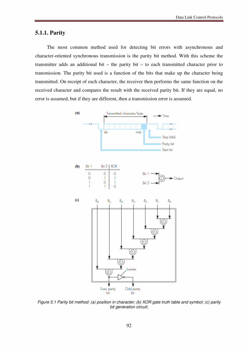
Data Link Control Protocols
92
5.1.1. Parity
The most common method used for detecting bit errors with asynchronous and
character-oriented synchronous transmission is the parity bit method. With this scheme the
transmitter adds an additional bit – the parity bit – to each transmitted character prior to
transmission. The parity bit used is a function of the bits that make up the character being
transmitted. On receipt of each character, the receiver then performs the same function on the
received character and compares the result with the received parity bit. If they are equal, no
error is assumed, but if they are different, then a transmission error is assumed.
Figure 5.1 Parity bit method: (a) position in character; (b) XOR gate truth table and symbol; (c) parity bit generation circuit;
Data Link Control Protocols
93
To compute the parity bit for a character, the number of 1 bits in the code for the
character are added together (modulo 2) and the parity bit is then chosen so that the total
number of 1 bits (including the parity bit itself) is either even – even parity – or odd – odd
parity. The principles of the scheme are shown in Figure 5.1.
The circuitry used to compute the parity bit for each character comprises a set of
exclusive-OR (XOR) gates connected as shown in Figure 5.1 (c). The XOR gate is also
known as a modulo-2 adder since, as shown by the truth table in part (b) of the figure, the
output of the exclusive-OR operation between two binary digits is the same as the addition of
the two digits without a carry bit. The least significant pair of bits are first XORed together
and the output of this gate is then XORed with the next (more significant) bit, and so on. The
output of the final gate is the required parity bit which is loaded into the transmit PISO
register prior to transmission of the character. Similarly, on receipt, the recomputed parity bit
is compared with the received parity bit. If it is different, this indicates that a transmission
error has been detected.
5.1.2. Block sum check
When blocks of characters (or bytes) are being transmitted, there is an increased
probability that a character (and hence the block) will contain a bit error. The probability of a
block containing an error is known as the block error rate. When blocks of characters
(frames) are being transmitted, we can achieve an extension to the error detecting capabilities
obtained from a single parity bit per character (byte) by using an additional set of parity bits
computed from the complete block of characters (bytes) in the frame. With this method, each
character (byte) in the frame is assigned a parity bit as before (transverse or row parity). In
addition, an extra bit is computed for each bit position (longitudinal or column parity) in the
complete frame. The resulting set of parity bits for each column is referred to as the block
(sum) check character since each bit making up the character is the modulo-2 sum of all the
bits in the corresponding column.
The example in Figure 5.2(a) uses odd parity for the row parity bits and even parity for
the column parity bits, and assumes that the frame contains printable characters only.
We can deduce from this example that although two bit errors in a character will escape
the row parity check, they will be detected by the corresponding column parity check. This is
true, of course, only if no two bit errors occur in the same column at the same time. Clearly,
the probability of this occurring is much less than the probability of two bit errors in a single
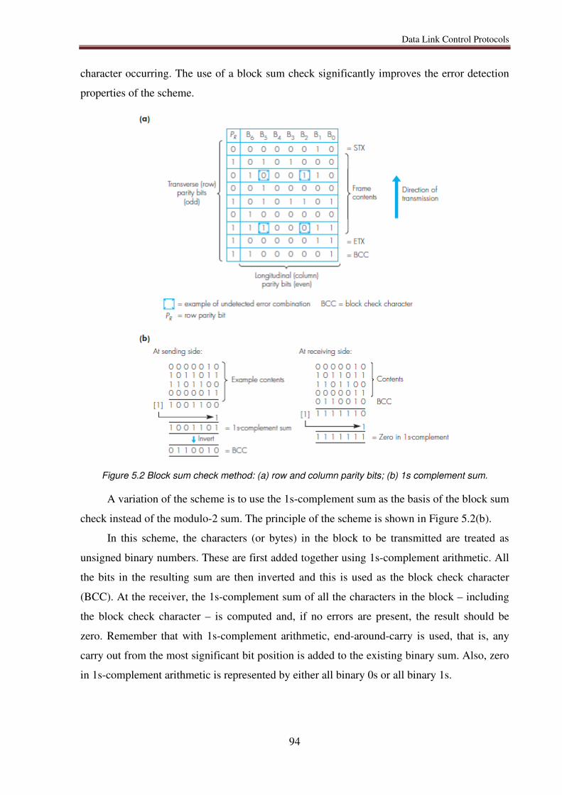
Data Link Control Protocols
94
character occurring. The use of a block sum check significantly improves the error detection
properties of the scheme.
Figure 5.2 Block sum check method: (a) row and column parity bits; (b) 1s complement sum.
A variation of the scheme is to use the 1s-complement sum as the basis of the block sum
check instead of the modulo-2 sum. The principle of the scheme is shown in Figure 5.2(b).
In this scheme, the characters (or bytes) in the block to be transmitted are treated as
unsigned binary numbers. These are first added together using 1s-complement arithmetic. All
the bits in the resulting sum are then inverted and this is used as the block check character
(BCC). At the receiver, the 1s-complement sum of all the characters in the block – including
the block check character – is computed and, if no errors are present, the result should be
zero. Remember that with 1s-complement arithmetic, end-around-carry is used, that is, any
carry out from the most significant bit position is added to the existing binary sum. Also, zero
in 1s-complement arithmetic is represented by either all binary 0s or all binary 1s.
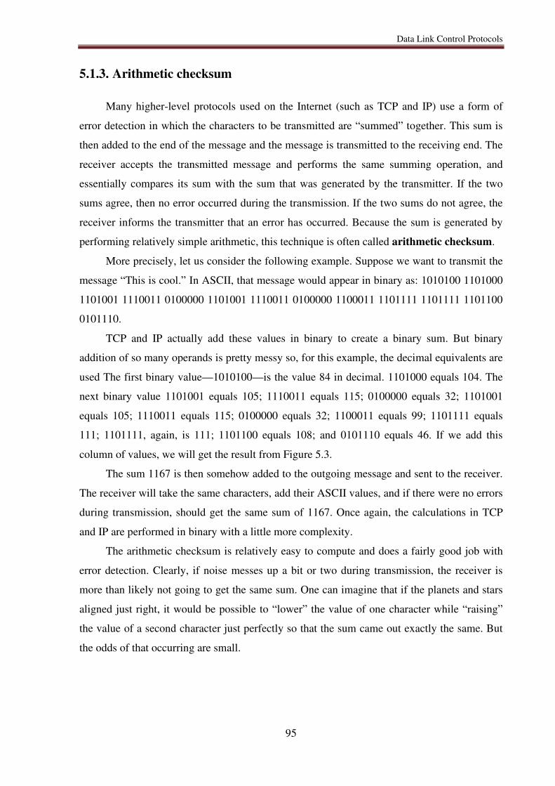
Data Link Control Protocols
95
5.1.3. Arithmetic checksum
Many higher-level protocols used on the Internet (such as TCP and IP) use a form of
error detection in which the characters to be transmitted are “summed” together. This sum is
then added to the end of the message and the message is transmitted to the receiving end. The
receiver accepts the transmitted message and performs the same summing operation, and
essentially compares its sum with the sum that was generated by the transmitter. If the two
sums agree, then no error occurred during the transmission. If the two sums do not agree, the
receiver informs the transmitter that an error has occurred. Because the sum is generated by
performing relatively simple arithmetic, this technique is often called arithmetic checksum.
More precisely, let us consider the following example. Suppose we want to transmit the
message “This is cool.” In ASCII, that message would appear in binary as: 1010100 1101000
1101001 1110011 0100000 1101001 1110011 0100000 1100011 1101111 1101111 1101100
0101110.
TCP and IP actually add these values in binary to create a binary sum. But binary
addition of so many operands is pretty messy so, for this example, the decimal equivalents are
used The first binary value—1010100—is the value 84 in decimal. 1101000 equals 104. The
next binary value 1101001 equals 105; 1110011 equals 115; 0100000 equals 32; 1101001
equals 105; 1110011 equals 115; 0100000 equals 32; 1100011 equals 99; 1101111 equals
111; 1101111, again, is 111; 1101100 equals 108; and 0101110 equals 46. If we add this
column of values, we will get the result from Figure 5.3.
The sum 1167 is then somehow added to the outgoing message and sent to the receiver.
The receiver will take the same characters, add their ASCII values, and if there were no errors
during transmission, should get the same sum of 1167. Once again, the calculations in TCP
and IP are performed in binary with a little more complexity.
The arithmetic checksum is relatively easy to compute and does a fairly good job with
error detection. Clearly, if noise messes up a bit or two during transmission, the receiver is
more than likely not going to get the same sum. One can imagine that if the planets and stars
aligned just right, it would be possible to “lower” the value of one character while “raising”
the value of a second character just perfectly so that the sum came out exactly the same. But
the odds of that occurring are small.
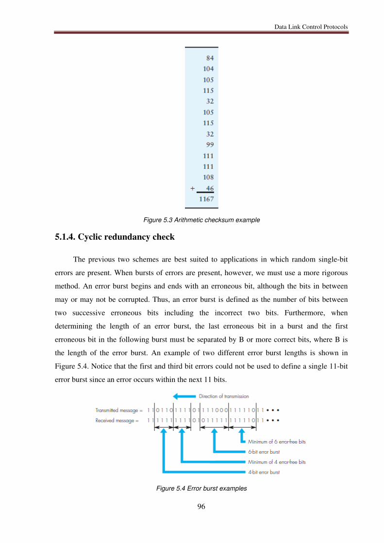
Data Link Control Protocols
96
Figure 5.3 Arithmetic checksum example
5.1.4. Cyclic redundancy check
The previous two schemes are best suited to applications in which random single-bit
errors are present. When bursts of errors are present, however, we must use a more rigorous
method. An error burst begins and ends with an erroneous bit, although the bits in between
may or may not be corrupted. Thus, an error burst is defined as the number of bits between
two successive erroneous bits including the incorrect two bits. Furthermore, when
determining the length of an error burst, the last erroneous bit in a burst and the first
erroneous bit in the following burst must be separated by B or more correct bits, where B is
the length of the error burst. An example of two different error burst lengths is shown in
Figure 5.4. Notice that the first and third bit errors could not be used to define a single 11-bit
error burst since an error occurs within the next 11 bits.
Figure 5.4 Error burst examples
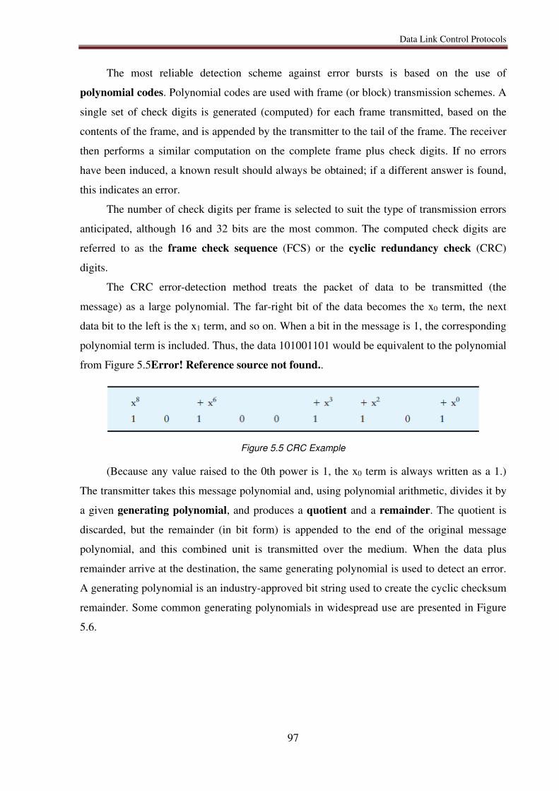
Data Link Control Protocols
97
The most reliable detection scheme against error bursts is based on the use of
polynomial codes. Polynomial codes are used with frame (or block) transmission schemes. A
single set of check digits is generated (computed) for each frame transmitted, based on the
contents of the frame, and is appended by the transmitter to the tail of the frame. The receiver
then performs a similar computation on the complete frame plus check digits. If no errors
have been induced, a known result should always be obtained; if a different answer is found,
this indicates an error.
The number of check digits per frame is selected to suit the type of transmission errors
anticipated, although 16 and 32 bits are the most common. The computed check digits are
referred to as the frame check sequence (FCS) or the cyclic redundancy check (CRC)
digits.
The CRC error-detection method treats the packet of data to be transmitted (the
message) as a large polynomial. The far-right bit of the data becomes the x0 term, the next
data bit to the left is the x1 term, and so on. When a bit in the message is 1, the corresponding
polynomial term is included. Thus, the data 101001101 would be equivalent to the polynomial
from Figure 5.5Error! Reference source not found..
Figure 5.5 CRC Example
(Because any value raised to the 0th power is 1, the x0 term is always written as a 1.)
The transmitter takes this message polynomial and, using polynomial arithmetic, divides it by
a given generating polynomial, and produces a quotient and a remainder. The quotient is
discarded, but the remainder (in bit form) is appended to the end of the original message
polynomial, and this combined unit is transmitted over the medium. When the data plus
remainder arrive at the destination, the same generating polynomial is used to detect an error.
A generating polynomial is an industry-approved bit string used to create the cyclic checksum
remainder. Some common generating polynomials in widespread use are presented in Figure
5.6.
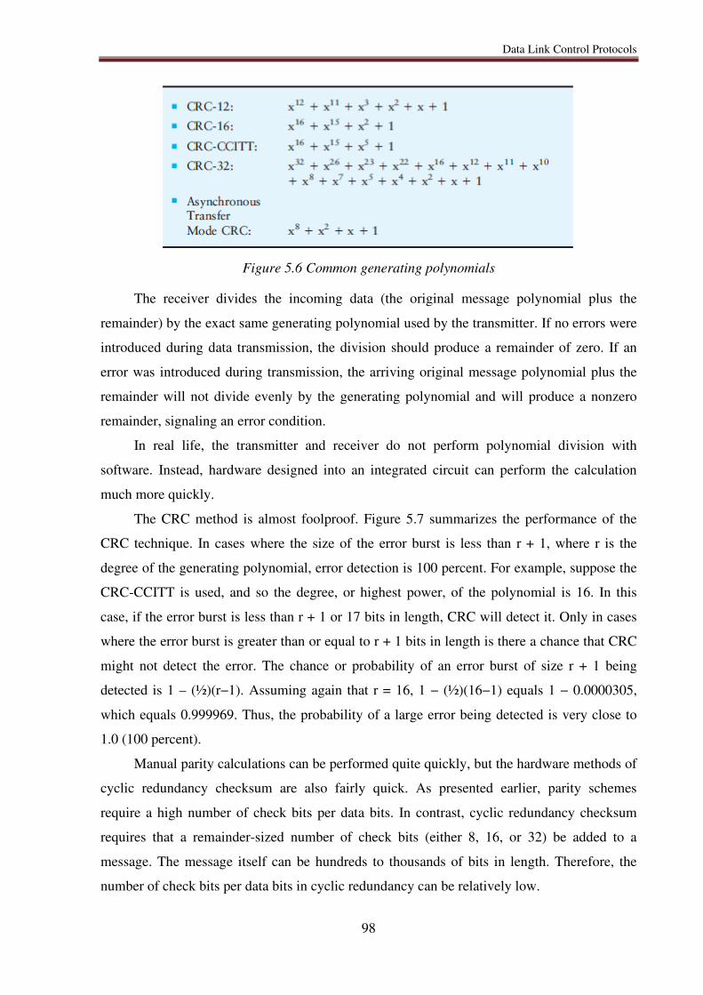
Data Link Control Protocols
98
Figure 5.6 Common generating polynomials
The receiver divides the incoming data (the original message polynomial plus the
remainder) by the exact same generating polynomial used by the transmitter. If no errors were
introduced during data transmission, the division should produce a remainder of zero. If an
error was introduced during transmission, the arriving original message polynomial plus the
remainder will not divide evenly by the generating polynomial and will produce a nonzero
remainder, signaling an error condition.
In real life, the transmitter and receiver do not perform polynomial division with
software. Instead, hardware designed into an integrated circuit can perform the calculation
much more quickly.
The CRC method is almost foolproof. Figure 5.7 summarizes the performance of the
CRC technique. In cases where the size of the error burst is less than r + 1, where r is the
degree of the generating polynomial, error detection is 100 percent. For example, suppose the
CRC-CCITT is used, and so the degree, or highest power, of the polynomial is 16. In this
case, if the error burst is less than r + 1 or 17 bits in length, CRC will detect it. Only in cases
where the error burst is greater than or equal to r + 1 bits in length is there a chance that CRC
might not detect the error. The chance or probability of an error burst of size r + 1 being
detected is 1 – (½)(r−1). Assuming again that r = 16, 1 − (½)(16−1) equals 1 − 0.0000305,
which equals 0.999969. Thus, the probability of a large error being detected is very close to
1.0 (100 percent).
Manual parity calculations can be performed quite quickly, but the hardware methods of
cyclic redundancy checksum are also fairly quick. As presented earlier, parity schemes
require a high number of check bits per data bits. In contrast, cyclic redundancy checksum
requires that a remainder-sized number of check bits (either 8, 16, or 32) be added to a
message. The message itself can be hundreds to thousands of bits in length. Therefore, the
number of check bits per data bits in cyclic redundancy can be relatively low.
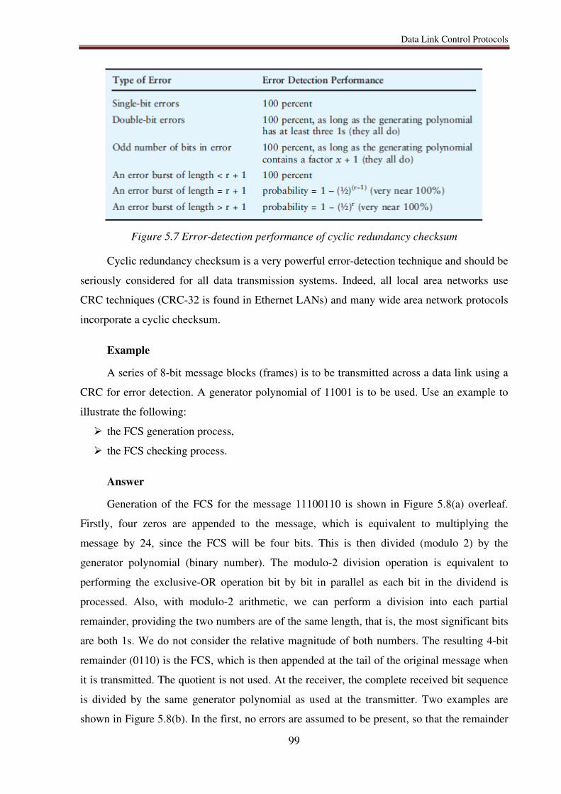
Data Link Control Protocols
99
Figure 5.7 Error-detection performance of cyclic redundancy checksum
Cyclic redundancy checksum is a very powerful error-detection technique and should be
seriously considered for all data transmission systems. Indeed, all local area networks use
CRC techniques (CRC-32 is found in Ethernet LANs) and many wide area network protocols
incorporate a cyclic checksum.
Example
A series of 8-bit message blocks (frames) is to be transmitted across a data link using a
CRC for error detection. A generator polynomial of 11001 is to be used. Use an example to
illustrate the following:
the FCS generation process,
the FCS checking process.
Answer
Generation of the FCS for the message 11100110 is shown in Figure 5.8(a) overleaf.
Firstly, four zeros are appended to the message, which is equivalent to multiplying the
message by 24, since the FCS will be four bits. This is then divided (modulo 2) by the
generator polynomial (binary number). The modulo-2 division operation is equivalent to
performing the exclusive-OR operation bit by bit in parallel as each bit in the dividend is
processed. Also, with modulo-2 arithmetic, we can perform a division into each partial
remainder, providing the two numbers are of the same length, that is, the most significant bits
are both 1s. We do not consider the relative magnitude of both numbers. The resulting 4-bit
remainder (0110) is the FCS, which is then appended at the tail of the original message when
it is transmitted. The quotient is not used. At the receiver, the complete received bit sequence
is divided by the same generator polynomial as used at the transmitter. Two examples are
shown in Figure 5.8(b). In the first, no errors are assumed to be present, so that the remainder
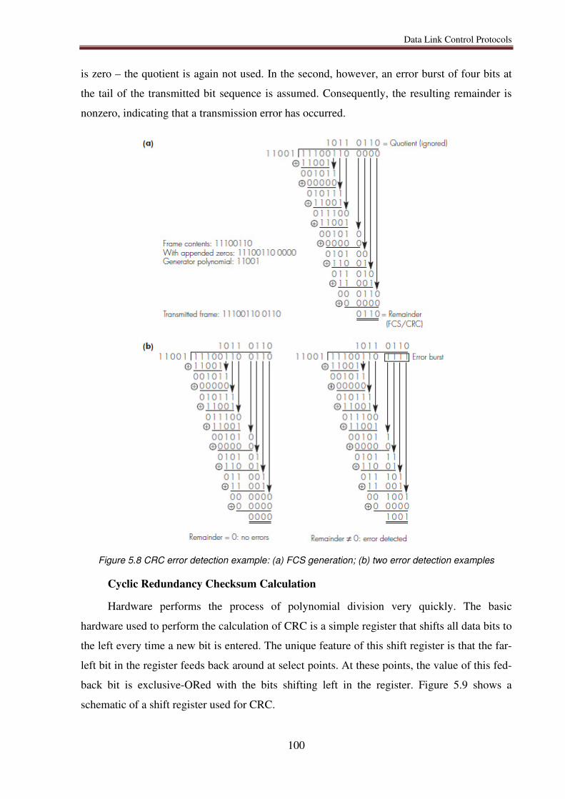
Data Link Control Protocols
100
is zero – the quotient is again not used. In the second, however, an error burst of four bits at
the tail of the transmitted bit sequence is assumed. Consequently, the resulting remainder is
nonzero, indicating that a transmission error has occurred.
Figure 5.8 CRC error detection example: (a) FCS generation; (b) two error detection examples
Cyclic Redundancy Checksum Calculation
Hardware performs the process of polynomial division very quickly. The basic
hardware used to perform the calculation of CRC is a simple register that shifts all data bits to
the left every time a new bit is entered. The unique feature of this shift register is that the far-
left bit in the register feeds back around at select points. At these points, the value of this fed-
back bit is exclusive-ORed with the bits shifting left in the register. Figure 5.9 shows a
schematic of a shift register used for CRC.
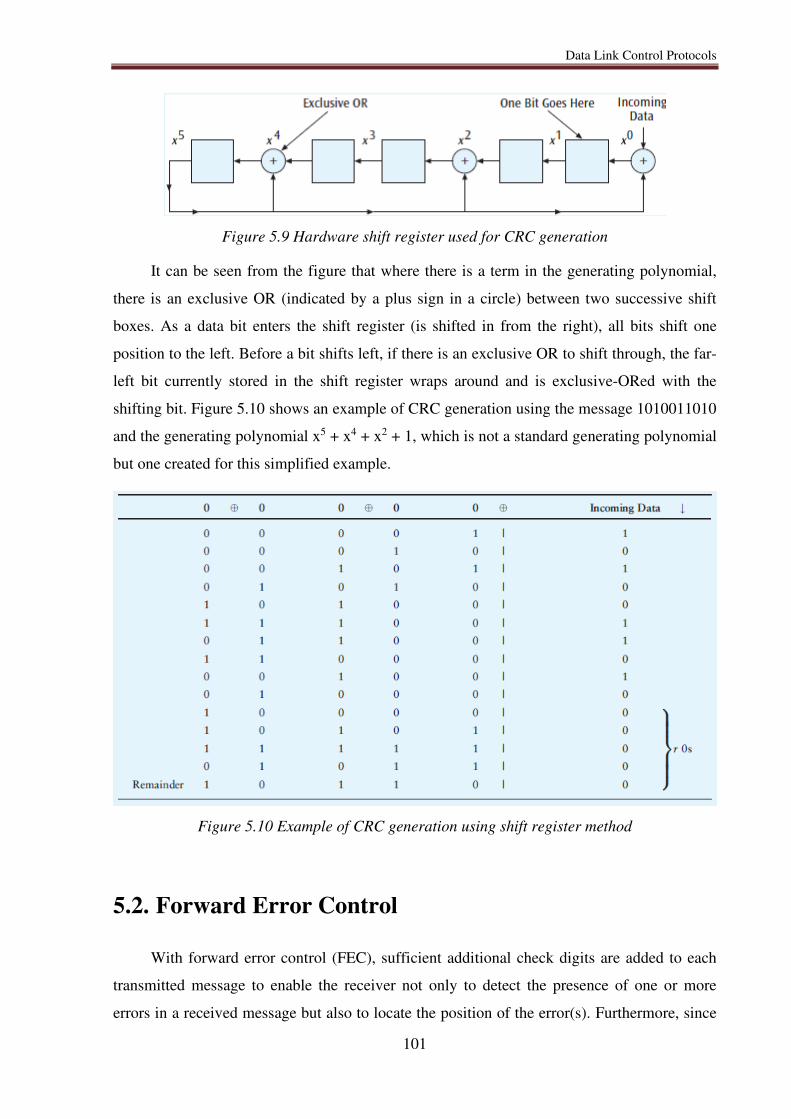
Data Link Control Protocols
101
Figure 5.9 Hardware shift register used for CRC generation
It can be seen from the figure that where there is a term in the generating polynomial,
there is an exclusive OR (indicated by a plus sign in a circle) between two successive shift
boxes. As a data bit enters the shift register (is shifted in from the right), all bits shift one
position to the left. Before a bit shifts left, if there is an exclusive OR to shift through, the far-
left bit currently stored in the shift register wraps around and is exclusive-ORed with the
shifting bit. Figure 5.10 shows an example of CRC generation using the message 1010011010
and the generating polynomial x5 + x4 + x2 + 1, which is not a standard generating polynomial
but one created for this simplified example.
Figure 5.10 Example of CRC generation using shift register method
5.2. Forward Error Control
With forward error control (FEC), sufficient additional check digits are added to each
transmitted message to enable the receiver not only to detect the presence of one or more
errors in a received message but also to locate the position of the error(s). Furthermore, since
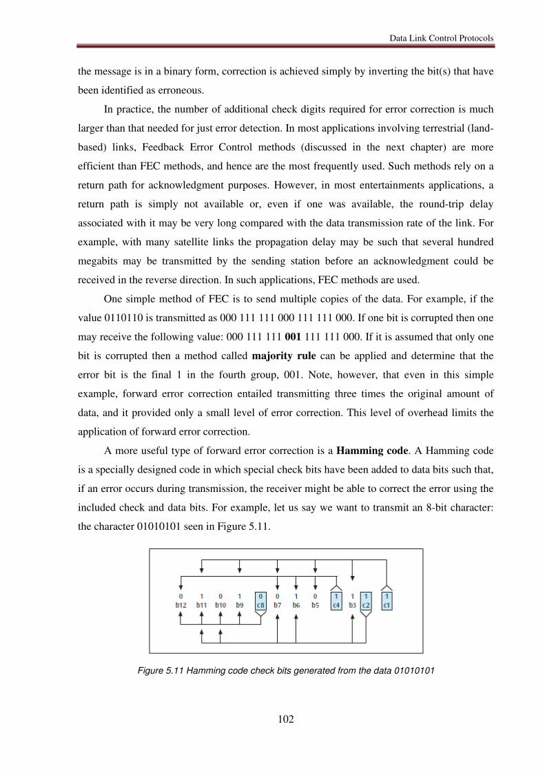
Data Link Control Protocols
102
the message is in a binary form, correction is achieved simply by inverting the bit(s) that have
been identified as erroneous.
In practice, the number of additional check digits required for error correction is much
larger than that needed for just error detection. In most applications involving terrestrial (land-
based) links, Feedback Error Control methods (discussed in the next chapter) are more
efficient than FEC methods, and hence are the most frequently used. Such methods rely on a
return path for acknowledgment purposes. However, in most entertainments applications, a
return path is simply not available or, even if one was available, the round-trip delay
associated with it may be very long compared with the data transmission rate of the link. For
example, with many satellite links the propagation delay may be such that several hundred
megabits may be transmitted by the sending station before an acknowledgment could be
received in the reverse direction. In such applications, FEC methods are used.
One simple method of FEC is to send multiple copies of the data. For example, if the
value 0110110 is transmitted as 000 111 111 000 111 111 000. If one bit is corrupted then one
may receive the following value: 000 111 111 001 111 111 000. If it is assumed that only one
bit is corrupted then a method called majority rule can be applied and determine that the
error bit is the final 1 in the fourth group, 001. Note, however, that even in this simple
example, forward error correction entailed transmitting three times the original amount of
data, and it provided only a small level of error correction. This level of overhead limits the
application of forward error correction.
A more useful type of forward error correction is a Hamming code. A Hamming code
is a specially designed code in which special check bits have been added to data bits such that,
if an error occurs during transmission, the receiver might be able to correct the error using the
included check and data bits. For example, let us say we want to transmit an 8-bit character:
the character 01010101 seen in Figure 5.11.
Figure 5.11 Hamming code check bits generated from the data 01010101
Data Link Control Protocols
103
Let us number the bits of this character b12, b11, b10, b9, b7, b6, b5, and b3. (We will
number the bits from right to left, leaving spaces for the soon-to-be-added check bits.) Now
add to these data bits the following check bits: c8, c4, c2, and c1, where c8 generates a simple
even parity for bits b12, b11, b10, and b9. The check bit c4 will generate a simple even parity
for bits b12, b7, b6, and b5. Check bit c2 will generate a simple even parity for bits b11, b10,
b7, b6, and b3. Finally, c1 will generate a simple even parity for bits b11, b9, b7, b5, and b3.
Note that each check bit here is checking different sequences of data bits.
Let us take a closer look at how each of the Hamming code check bits in Figure 5.11
works. Note that c8 “covers” bits b12, b11, b10, and b9, which are 0101. If we generate an
even parity bit based on those four bits, we would generate a 0 (there are an even number of
1s). Thus, c8 equals 0. c4 covers b12, b7, b6, and b5, which are 0010, so c4 equals 1. c2
covers b11, b10, b7, b6, and b3, which are 10011, so c2 equals 1. c1 covers b11, b9, b7, b5,
and b3, which are 11001, so c1 equals 1. Consequently, if we have the data 01010101, we
would generate the check bits 0111, as shown in Figure 5.11.
This 12-bit character is now transmitted to the receiver. The receiver accepts the bits
and performs the four parity checks on the check bits c8, c4, c2, and c1. If nothing happened
to the 12-bit character during transmission, all four parity checks should result in no error. But
what would happen if one of the bits were corrupted and somehow ends up the opposite
value? For example, what if bit b9 is corrupted? With the corrupted b9, we would now have
the string 010000101111. The receiver would perform the four parity checks, but this time
there would be parity errors. More precisely, because c8 checks b12, b11, b10, b9, and c8
(01000), there would be a parity error. As you can see, there is an odd number of 1s in the
data string, but the check bit is returning a 0. c4 checks b12, b7, b6, b5, and c4 (00101) and,
thus, would produce no parity error. c2 checks b11, b10, b7, b6, b3, and c2 (100111), and
would produce no parity error. c1 checks bits b11, b9, b7, b5, b3, and c1 (100011), which
would result in a parity error. Notice that if we examine just the check bits and denote a 1 if
there is a parity error and a 0 if there is no parity error, we would get 1001 (c8 error, c4 no
error, c2 no error, c1 error). 1001 is binary for 9, telling us that the bit in error is in the ninth
position.
Despite the additional costs of using forward error correction, are there applications that
would benefit from the use of this technology? Two major groups of applications can in fact
reap a benefit: digital television transmissions and applications that send data over very long
distances. Digital television signals use advanced forms of forward error correction called
Reed-Solomon codes and Trellis encoding. Note that it is not possible to ask for
Data Link Control Protocols
104
retransmission of a TV signal if there is an error. It would be too late! The data needs to be
delivered in real time, thus the need for forward error correction. In the second example, if
data has to be sent over a long distance, it is costly time-wise and money-wise to retransmit a
packet that arrived in error. For example, the time required for NASA to send a message to a
Martian probe is several minutes. If the data arrives garbled, it will be another several minutes
before the negative acknowledgment is received, and another several minutes before the data
can be retransmitted. If a large number of data packets arrive garbled, transmitting data to
Mars could be a very long, tedious process.
5.3. Feedback Error Control
Even very powerful error-correcting codes may not be able to correct all errors that arise
in a communications channel. Also, often the error rate of the link is extremely small and the
additional bits added by the error-correcting codes are not used most of the time thus limiting
the amount of actual data that can be transmitted. Consequently, many data communications
links provide a further error control mechanism, in which errors in data are detected and the
data is retransmitted. This procedure is known as feedback error control and it involves using
a mechanism to detect errors at the receive end of a link and then returning a message to the
transmitter requesting the retransmission of a block (or blocks) of data. The process of
retransmitting the data has traditionally been known as Automatic Repeat Request (ARQ). A
number of derivatives of the basic scheme are possible, the choice being determined by the
relative importance assigned to the use of buffer storage compared with the efficiency of
utilization of the available transmission capacity. The two most common alternatives are idle
RQ (send-and-wait) and continuous RQ, the latter employing either a selective
retransmission strategy or a go-back-N mechanism. Each of these schemes will now be
considered separately.
5.3.1. Idle RQ
In order to discriminate between the sender (source) and receiver (destination) of data
frames – more generally referred to as information or I-frames – the terms primary (P) and
secondary (S) are used respectively. The idle RQ protocol operates in a half-duplex mode
since the primary, after sending an I-frame, waits until it receives a response from the
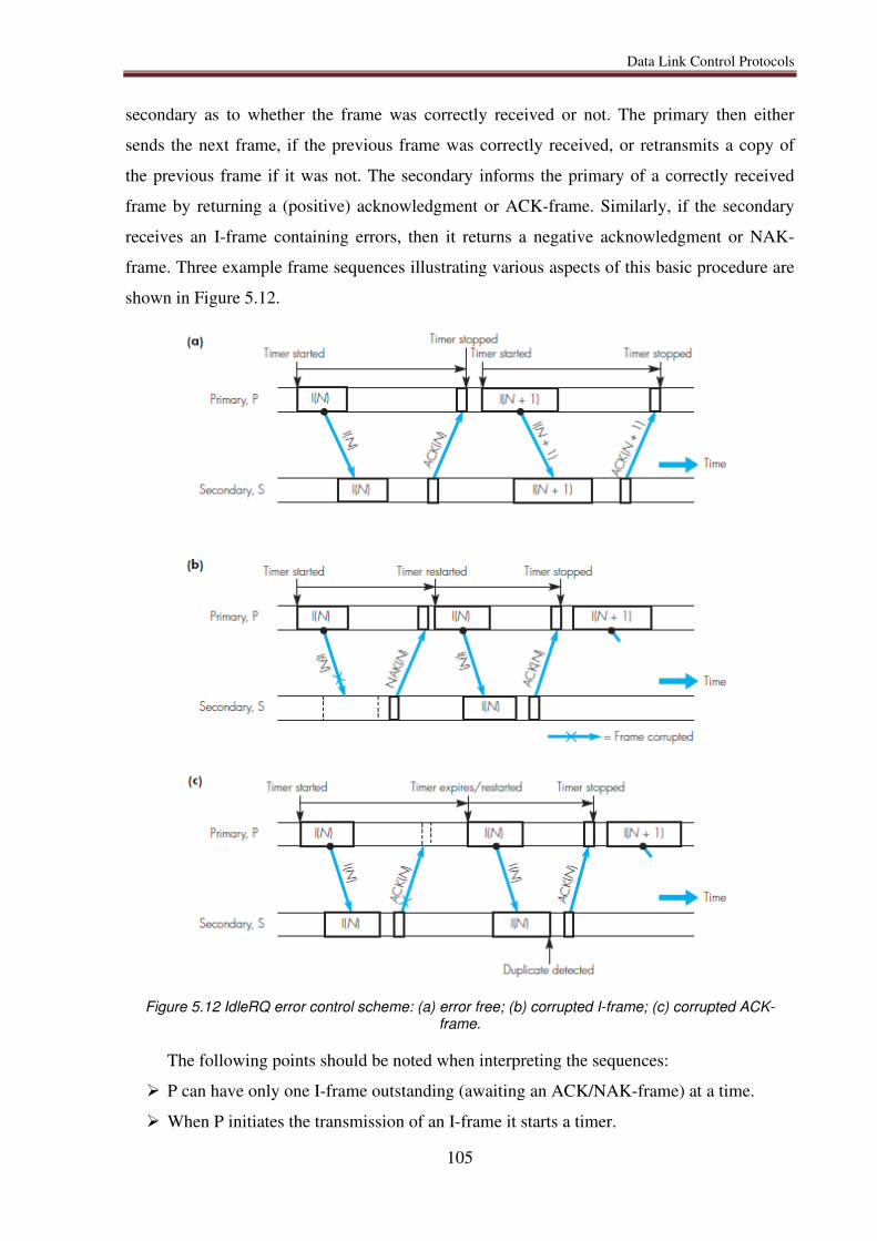
Data Link Control Protocols
105
secondary as to whether the frame was correctly received or not. The primary then either
sends the next frame, if the previous frame was correctly received, or retransmits a copy of
the previous frame if it was not. The secondary informs the primary of a correctly received
frame by returning a (positive) acknowledgment or ACK-frame. Similarly, if the secondary
receives an I-frame containing errors, then it returns a negative acknowledgment or NAK-
frame. Three example frame sequences illustrating various aspects of this basic procedure are
shown in Figure 5.12.
Figure 5.12 IdleRQ error control scheme: (a) error free; (b) corrupted I-frame; (c) corrupted ACK-frame.
The following points should be noted when interpreting the sequences:
P can have only one I-frame outstanding (awaiting an ACK/NAK-frame) at a time.
When P initiates the transmission of an I-frame it starts a timer.
Data Link Control Protocols
106
On receipt of an error-free I-frame, S returns an ACK-frame to P and, on receipt of this,
P stops the timer for this frame and proceeds to send the next frame – part (a).
On receipt of an I-frame containing transmission errors, S discards the frame and returns
a NAK-frame to P which then sends another copy of the frame and restarts the timer –
part (b).
If P does not receive an ACK- (or NAK-) frame within the timeout interval, P
retransmits the I-frame currently waiting acknowledgment – part (c). However, since in
this example it is an ACK-frame that is corrupted, S detects that the next frame it
receives is a duplicate copy of the previous error-free frame it received rather than a
new frame. Hence S discards the duplicate and, to enable P to resynchronize, returns a
second ACK-frame for it. This procedure repeats until either an error-free copy of the
frame is received or a defined number of retries is reached in which case the network
layer in P would be informed of this.
As presented in the figure, in order for S to determine when a duplicate is received, each
frame transmitted by P contains a unique identifier known as the send sequence number N(S)
(N, N+1, and so on) within it. Also, S retains a record of the sequence number contained
within the last I-frame it received without errors and, if the two are the same, this indicates a
duplicate. The sequence number in each ACK- and NAK-frame is known as the receive
sequence number N(R) and, since P must wait for an ACK- or NAK-frame after sending each
I-frame, the scheme is known also as send-and-wait or sometimes stop-and-wait.
Alternatively, since only a single frame is being transferred at a time, only two sequence
numbers are required. Normally, just a single bit is used and this alternates between 0 and 1.
Hence the scheme is known also as the alternating bit protocol and an example application is
in the Bluetooth wireless network
5.3.2. Continuous RQ
With a continuous RQ error control scheme, link utilization is much improved at the
expense of increased buffer storage requirements. As it shall be seen, a duplex link is required
for its implementation. An example illustrating the transmission of a sequence of I-frames and
their returned ACK-frames is shown in Figure 5.13.
Data Link Control Protocols
107
Figure 5.13 Continuous RQ frame sequence without transmission errors.
When interpreting the operation of the scheme the following points should be noted:
P sends I-frames continuously without waiting for an ACK-frame to be returned.
Since more than one I-frame is awaiting acknowledgment, P retains a copy of each I-
frame transmitted in a retransmission list that operates on a FIFO queue discipline.
S returns an ACK-frame for each correctly received I-frame.
Each I-frame contains a unique identifier which is returned in the corresponding ACK-
frame.
On receipt of an ACK-frame, the corresponding I-frame is removed from the
retransmission list by P.
Frames received free of errors are placed in the link receive list to await processing.
On receipt of the next in-sequence I-frame expected, S delivers the information content
within the frame to the upper network layer immediately it has processed the frame.
which indicates the send sequence number N(S) to be allocated to the next
I-frame to be transmitted. Also, S must maintain a receive sequence variable
V(R), which indicates the next in-sequence I-frame it is waiting for.
Data Link Control Protocols
108
The frame sequence shown in Figure 5.13 assumes that no transmission errors occur.
When an error does occur, one of two retransmission strategies may be followed:
S detects and requests the retransmission of just those frames in the sequence that are
corrupted – selective retransmission (also known as selective reject).
S detects the receipt of an out-of-sequence I-frame and requests P to retransmit all
outstanding unacknowledged I-frames from the last correctly received, and hence
acknowledged, I-frame – go-back-N.
Note that with both continuous RQ schemes, corrupted frames are discarded and
retransmission requests are triggered only after the next error-free frame is received. Hence,
as with the idle RQ scheme, a timeout is applied to each frame transmitted to overcome the
possibility of a corrupted frame being the last in a sequence of new frames.
Selective retransmission
Two example frame sequence diagrams that illustrate the operation of the selective
repeat retransmission control scheme are shown in Figure 5.14.
The sequence shown in part (a) shows the effect of a corrupted I-frame being received
by S. The following points should be noted when interpreting the sequence:
An ACK-frame acknowledges all frames in the retransmission list up to and including
the I-frame with the sequence number the ACK contains.
Assume I-frame N+1 is corrupted.
S returns an ACK-frame for I-frame N.
When S receives I-frame N+2 it detects I-frame N+1 is missing from V(R) and hence
returns a NAK-frame containing the identifier of the missing I-frame N+1.
On receipt of NAK N+1, P interprets this as S is still awaiting I-frame N+1 and hence
retransmits it.
When P retransmits I-frame N+1 it enters the retransmission state.
When P is in the retransmission state, it suspends sending any new frames and sets a
timeout for the receipt of ACK N+1.
If the timeout expires, another copy of I-frame (N+1) is sent.
On receipt of ACK N+1 P leaves the retransmission state and resumes sending new
frames.
When S returns a NAK-frame it enters the retransmission state.
When S is in the retransmission state, the return of ACK-frames is suspended.
Data Link Control Protocols
109
Figure 5.14 Selective retransmission: (a) effect of corrupted I-frame; (b) effect of corrupted ACK-frame.
On receipt of I-frame N+1, S leaves the retransmission state and resumes returning
ACK-frames.
ACK N+1 acknowledges all frames up to and including frame N+4.
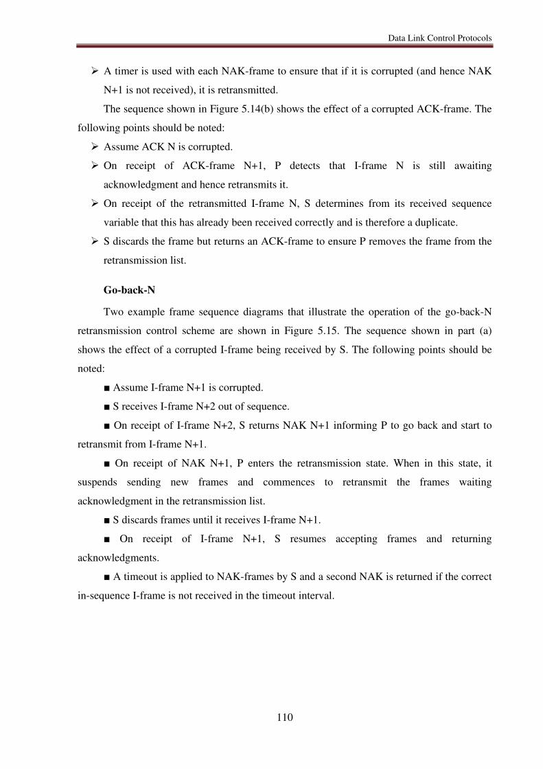
Data Link Control Protocols
110
A timer is used with each NAK-frame to ensure that if it is corrupted (and hence NAK
N+1 is not received), it is retransmitted.
The sequence shown in Figure 5.14(b) shows the effect of a corrupted ACK-frame. The
following points should be noted:
Assume ACK N is corrupted.
On receipt of ACK-frame N+1, P detects that I-frame N is still awaiting
acknowledgment and hence retransmits it.
On receipt of the retransmitted I-frame N, S determines from its received sequence
variable that this has already been received correctly and is therefore a duplicate.
S discards the frame but returns an ACK-frame to ensure P removes the frame from the
retransmission list.
Go-back-N
Two example frame sequence diagrams that illustrate the operation of the go-back-N
retransmission control scheme are shown in Figure 5.15. The sequence shown in part (a)
shows the effect of a corrupted I-frame being received by S. The following points should be
noted:
■ Assume I-frame N+1 is corrupted.
■ S receives I-frame N+2 out of sequence.
■ On receipt of I-frame N+2, S returns NAK N+1 informing P to go back and start to
retransmit from I-frame N+1.
■ On receipt of NAK N+1, P enters the retransmission state. When in this state, it
suspends sending new frames and commences to retransmit the frames waiting
acknowledgment in the retransmission list.
■ S discards frames until it receives I-frame N+1.
■ On receipt of I-frame N+1, S resumes accepting frames and returning
acknowledgments.
■ A timeout is applied to NAK-frames by S and a second NAK is returned if the correct
in-sequence I-frame is not received in the timeout interval.
Data Link Control Protocols
111
Figure 5.15 Go-back-N retransmission strategy: (a) corrupted I-frame; (b) corrupted ACK-frame.
The frame sequence shown in Figure 5.15(b) shows the effect of a corrupted ACK-
frame. Note that:
■ S receives each transmitted I-frame correctly.
Data Link Control Protocols
112
■ Assume ACK-frames N and N+1 are both corrupted.
■ On receipt of ACK-frame N+2, P detects that there are two outstanding I-frames in
the retransmission list (N and N+1).
■ Since it is an ACK-frame rather than a NAK-frame, P assumes that the two ACK-
frames for I-frames N and N+1 have both been corrupted and hence accepts ACK-frame N+2
as an acknowledgment for the outstanding frames.
In order to discriminate between the NAK-frames used in the two schemes, in the
selective repeat scheme a NAK is known as a selective reject and in the go-back-N scheme a
reject.
5.4. Flow control
Error control is only one component of a data link protocol. Another important and
related component is flow control. As the name implies, it is concerned with controlling the
rate of transmission of frames on a link so that the receiver always has sufficient buffer
storage resources to accept them prior to processing.
To control the flow of frames across a link, a mechanism known as a sliding window is
used. The approach is similar to the idle RQ control scheme in that it essentially sets a limit
on the number of I-frames that P may send before receiving an acknowledgment. P monitors
the number of outstanding (unacknowledged) I-frames currently held in the retransmission
list. If the destination side of the link is unable to pass on the frames sent to it, S stops
returning acknowledgment frames, the retransmission list at P builds up and this in turn can
be interpreted as a signal for P to stop transmitting further frames until acknowledgments start
to flow again.
To implement this scheme, a maximum limit is set on the number of I-frames that can
be awaiting acknowledgment and hence are outstanding in the retransmission list. This limit is
the send window, K for the link. If this is set to 1, the retransmission control scheme reverts
to idle RQ with a consequent drop in transmission efficiency. The limit is normally selected
so that, providing the destination is able to pass on or absorb all frames it receives, the send
window does not impair the flow of I-frames across the link. Factors such as the maximum
frame size, available buffer storage, link propagation delay, and transmission bit rate must all
be considered when selecting the send window.
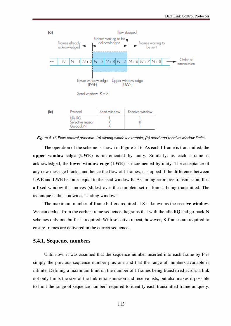
Data Link Control Protocols
113
Figure 5.16 Flow control principle: (a) sliding window example; (b) send and receive window limits.
The operation of the scheme is shown in Figure 5.16. As each I-frame is transmitted, the
upper window edge (UWE) is incremented by unity. Similarly, as each I-frame is
acknowledged, the lower window edge (LWE) is incremented by unity. The acceptance of
any new message blocks, and hence the flow of I-frames, is stopped if the difference between
UWE and LWE becomes equal to the send window K. Assuming error-free transmission, K is
a fixed window that moves (slides) over the complete set of frames being transmitted. The
technique is thus known as “sliding window”.
The maximum number of frame buffers required at S is known as the receive window.
We can deduct from the earlier frame sequence diagrams that with the idle RQ and go-back-N
schemes only one buffer is required. With selective repeat, however, K frames are required to
ensure frames are delivered in the correct sequence.
5.4.1. Sequence numbers
Until now, it was assumed that the sequence number inserted into each frame by P is
simply the previous sequence number plus one and that the range of numbers available is
infinite. Defining a maximum limit on the number of I-frames being transferred across a link
not only limits the size of the link retransmission and receive lists, but also makes it possible
to limit the range of sequence numbers required to identify each transmitted frame uniquely.
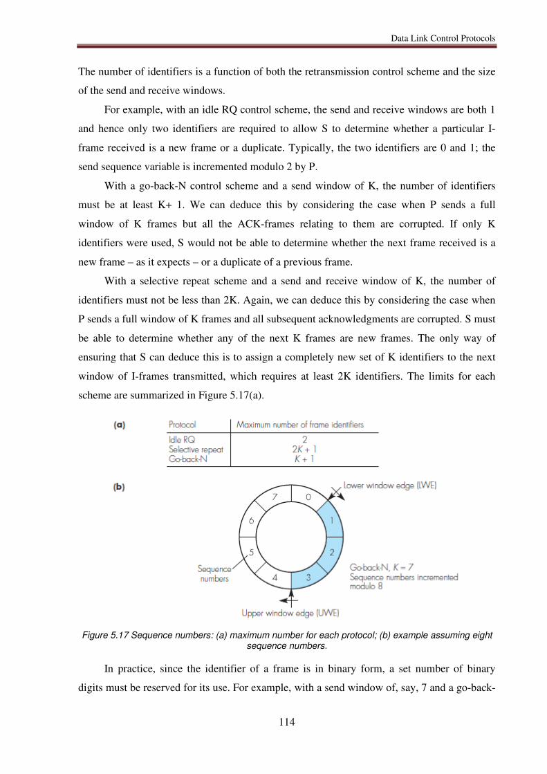
Data Link Control Protocols
114
The number of identifiers is a function of both the retransmission control scheme and the size
of the send and receive windows.
For example, with an idle RQ control scheme, the send and receive windows are both 1
and hence only two identifiers are required to allow S to determine whether a particular I-
frame received is a new frame or a duplicate. Typically, the two identifiers are 0 and 1; the
send sequence variable is incremented modulo 2 by P.
With a go-back-N control scheme and a send window of K, the number of identifiers
must be at least K+ 1. We can deduce this by considering the case when P sends a full
window of K frames but all the ACK-frames relating to them are corrupted. If only K
identifiers were used, S would not be able to determine whether the next frame received is a
new frame – as it expects – or a duplicate of a previous frame.
With a selective repeat scheme and a send and receive window of K, the number of
identifiers must not be less than 2K. Again, we can deduce this by considering the case when
P sends a full window of K frames and all subsequent acknowledgments are corrupted. S must
be able to determine whether any of the next K frames are new frames. The only way of
ensuring that S can deduce this is to assign a completely new set of K identifiers to the next
window of I-frames transmitted, which requires at least 2K identifiers. The limits for each
scheme are summarized in Figure 5.17(a).
Figure 5.17 Sequence numbers: (a) maximum number for each protocol; (b) example assuming eight sequence numbers.
In practice, since the identifier of a frame is in binary form, a set number of binary
digits must be reserved for its use. For example, with a send window of, say, 7 and a go-back-
Data Link Control Protocols
115
N control scheme, three binary digits are required for the send and receive sequence numbers
yielding eight possible identifiers: 0 through 7. The send and receive sequence variables are
then incremented modulo 8 by P and S respectively. This is illustrated in Figure 5.17(b).
5.4.2. Performance Issues
In this chapter, some of the performance issues related to the use of stop and wait and
sliding window flow control are examined.
Stop-and-Wait Flow Control
Let us determine the maximum potential efficiency of a half-duplex point-to-point line
using the stop-and-wait scheme. Suppose that a long message is to be sent as a sequence of
frames F1, F2, …, Fn in the following fashion:
Station S1 sends F1
Station S2 sends an acknowledgment.
Station S1 sends F2
Station S2 sends an acknowledgment.
…
Station S1 sends Fn
Station S2 sends an acknowledgment.
The total time to send the data, T, can be expressed as � = 9 × �c, where TF is the time
to send one frame and receive an acknowledgment. We can express TF as follows:
TF = tprop + tframe + tproc + tprop + tack + tproc
where
tprop = propagation time from S1 to S2
tframe = time to transmit a frame
tproc = processing time at each station to react to an incoming event
tack = time to transmit an acknowledgment
Let us assume that the processing time is relatively negligible, and that the
acknowledgment frame is very small compared to a data frame, both of which are reasonable
assumptions.
Then we can express the total time to send the data as
T = n(2tprop + tframe)
Data Link Control Protocols
116
Of that time, only 9 × 7����� is actually spent transmitting data and the rest is overhead.
The utilization, or efficiency, of the line is
d = 9 × 7�����9(27���� + 7�����) = 7�����27���� + 7����� By using the parameter � = 7���� 7�����⁄ (see chapter 3.4), the formula for the
efficiency becomes:
d = 11 + 2� This is the maximum possible utilization of the link. Because the frame contains
overhead bits, actual utilization is lower. The parameter a is constant if both tprop and tframe are
constants, which is typically the case: Fixed-length frames are often used for all except the
last frame in a sequence, and the propagation delay is constant for point-to-point links.
To get some insight into the previous equation, let us derive a different expression for a.
We have
� = AL<E�V�7;<9 7;D8�L�9)D;));<9 7;D8
(7.5)
The propagation time is equal to the distance d of the link divided by the velocity of
propagation V. For unguided transmission through air or space, V is the speed of light,
approximately 3 × 10% D/). For guided transmission, V is approximately 0.67 times the
speed of light for optical fiber and copper media. The transmission time is equal to the length
of the frame in bits, L, divided by the data rate R. Therefore,
� = B ⁄f +⁄ = B+f
Thus, for fixed-length frames, a is proportional to the data rate times the length of the
medium. A useful way of looking at a is that it represents the length of the medium in bits
[+ × (B ⁄ )] compared to the frame length (L).
Error-Free Sliding-Window Flow Control
For sliding-window flow control, the throughput on the line depends on both the
window size W and the value of a. For convenience, the frame transmission time is
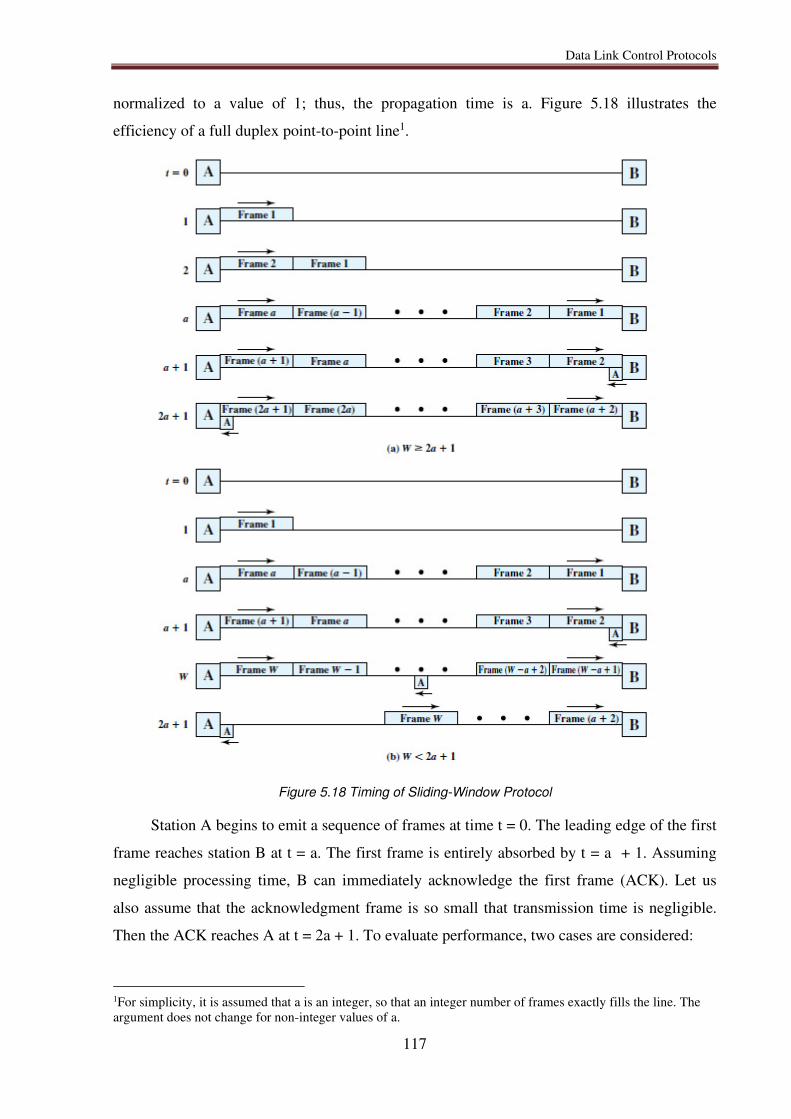
Data Link Control Protocols
117
normalized to a value of 1; thus, the propagation time is a. Figure 5.18 illustrates the
efficiency of a full duplex point-to-point line1.
Figure 5.18 Timing of Sliding-Window Protocol
Station A begins to emit a sequence of frames at time t = 0. The leading edge of the first
frame reaches station B at t = a. The first frame is entirely absorbed by t = a + 1. Assuming
negligible processing time, B can immediately acknowledge the first frame (ACK). Let us
also assume that the acknowledgment frame is so small that transmission time is negligible.
Then the ACK reaches A at t = 2a + 1. To evaluate performance, two cases are considered:
1For simplicity, it is assumed that a is an integer, so that an integer number of frames exactly fills the line. The argument does not change for non-integer values of a.
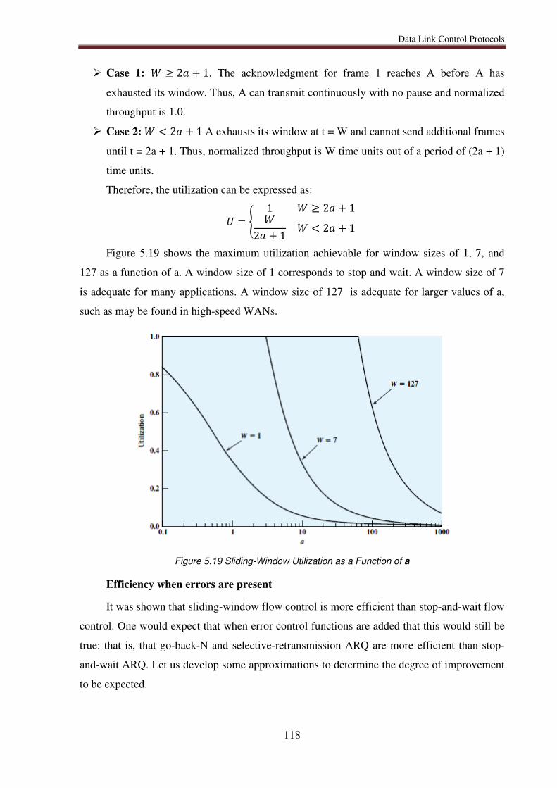
Data Link Control Protocols
118
Case 1: O ≥ 2� + 1. The acknowledgment for frame 1 reaches A before A has
exhausted its window. Thus, A can transmit continuously with no pause and normalized
throughput is 1.0.
Case 2: O < 2� + 1 A exhausts its window at t = W and cannot send additional frames
until t = 2a + 1. Thus, normalized throughput is W time units out of a period of (2a + 1)
time units.
Therefore, the utilization can be expressed as:
d = i 1 O ≥ 2� + 1O2� + 1 O < 2� + 1 Figure 5.19 shows the maximum utilization achievable for window sizes of 1, 7, and
127 as a function of a. A window size of 1 corresponds to stop and wait. A window size of 7
is adequate for many applications. A window size of 127 is adequate for larger values of a,
such as may be found in high-speed WANs.
Figure 5.19 Sliding-Window Utilization as a Function of a
Efficiency when errors are present
It was shown that sliding-window flow control is more efficient than stop-and-wait flow
control. One would expect that when error control functions are added that this would still be
true: that is, that go-back-N and selective-retransmission ARQ are more efficient than stop-
and-wait ARQ. Let us develop some approximations to determine the degree of improvement
to be expected.
Data Link Control Protocols
119
First, consider stop-and-wait ARQ. With no errors, the maximum utilization is 1 (1 + 2�)⁄ .If We want to account for the possibility that some frames are repeated because
of bit errors. To start, note that the utilization U can be defined as
d = ����
where
Tf = time for transmitter to emit a single frame
Tt = total time that line is engaged in the transmission of a single frame
If errors occur, the previous equation is modified to:
d = ��*���
Where Nr is the expected number of transmissions of a frame. Thus, for stop-and-wait
ARQ, we have
d = 1*�(1 + 2�)
A simple expression for Nr can be derived by considering the probability P that a single
frame is in error. If we assume that ACKs and NAKs are never in error, the probability that it
will take exactly k attempts to transmit a frame successfully is Pk-1(1 - P). That is, we have (k
- 1) unsuccessful attempts followed by one successful attempt; the probability of this
occurring is just the product of the probability of the individual events occurring. Then2
*� = j(; × Pr [; 7L�9)D;));<9)])o
p4= j(;A'4(1 − A))
op4
= 11 − A
So, for stop-and-wait we have:
d = 1 − A(1 + 2�)
For selective-retransmission ARQ, we can use the same reasoning as applied to stop-
and-wait ARQ. That is, the error-free equations must be divided by Nr. Again, *� =1 (1 − A)⁄ , so we have:
d = i 1 − A O ≥ 2� + 1O(1 − A)2� + 1 O < 2� + 1
2 This derivation uses the equality ∑ ;r'4op4 = 4(4's)J for -1 < X < 1
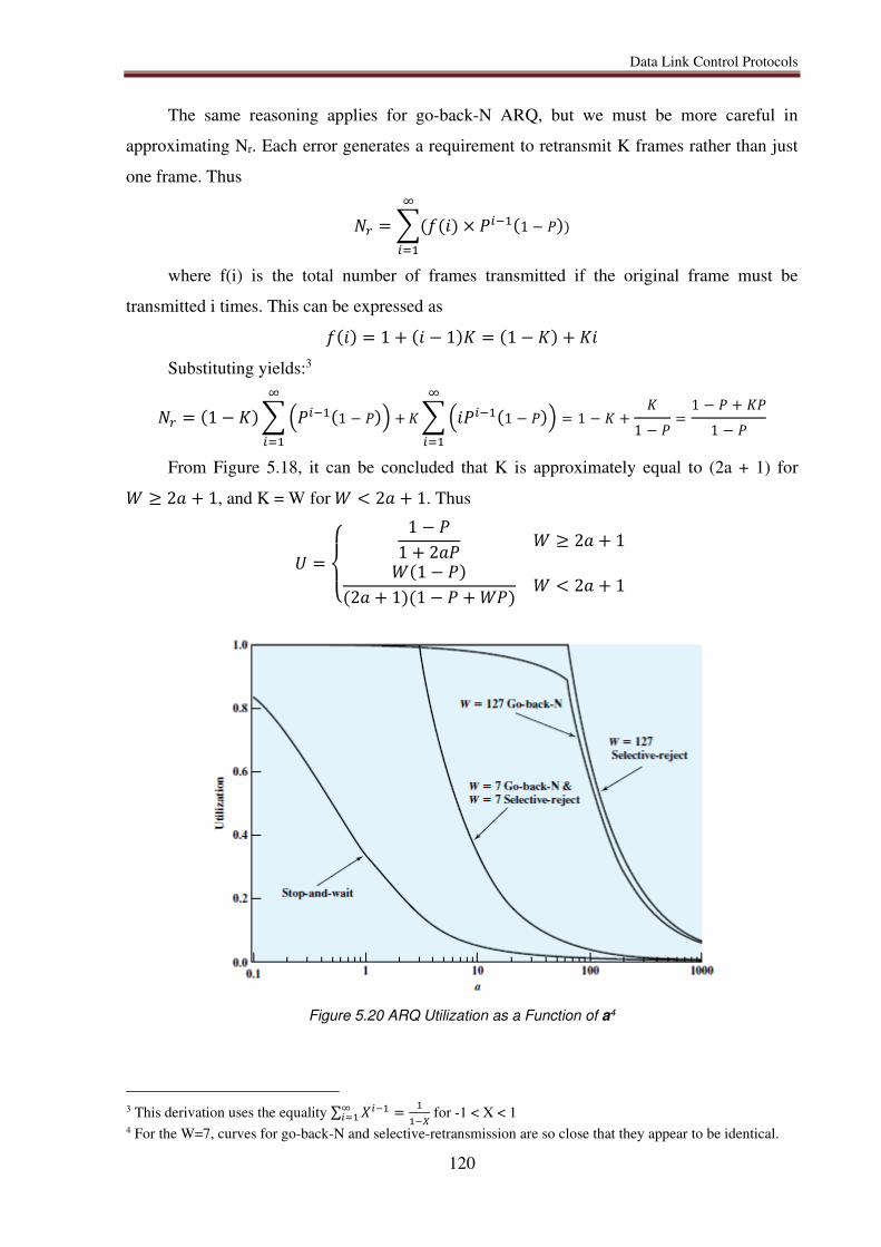
Data Link Control Protocols
120
The same reasoning applies for go-back-N ARQ, but we must be more careful in
approximating Nr. Each error generates a requirement to retransmit K frames rather than just
one frame. Thus
*� = j(G(;) × A'4(1 − A))o
p4
where f(i) is the total number of frames transmitted if the original frame must be
transmitted i times. This can be expressed as
G(;) = 1 + (; − 1)t = (1 − t) + t; Substituting yields:3
*� = (1 − t) j uA'4(1 − A)v +o
p4t j u;A'4(1 − A)vo
p4= 1 − t + t1 − A = 1 − A + tA1 − A
From Figure 5.18, it can be concluded that K is approximately equal to (2a + 1) for O ≥ 2� + 1, and K = W for O < 2� + 1. Thus
d =⎩⎨⎧ 1 − A1 + 2�A O ≥ 2� + 1
O(1 − A)(2� + 1)(1 − A + OA) O < 2� + 1
Figure 5.20 ARQ Utilization as a Function of a4
3 This derivation uses the equality ∑ r'4op4 = 44's for -1 < X < 1 4 For the W=7, curves for go-back-N and selective-retransmission are so close that they appear to be identical.
Data Link Control Protocols
121
Note that for W = 1 both selective-retransmission and go-back-N ARQ reduce to stop
and wait.
Figure 5.20 compares these three error control techniques for a value of P = 10-3 This
figure and the equations are only approximations. For example, we have ignored errors in
acknowledgment frames and, in the case of go-back-N, errors in retransmitted frames other
than the frame initially in error. However, the results do give an indication of the relative
performance of the three techniques.
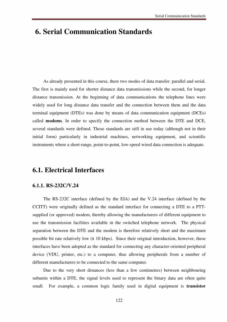
Serial Communication Standards
122
6. Serial Communication Standards
As already presented in this course, there two modes of data transfer: parallel and serial.
The first is mainly used for shorter distance data transmissions while the second, for longer
distance transmission. At the beginning of data communications the telephone lines were
widely used for long distance data transfer and the connection between them and the data
terminal equipment (DTEs) was done by means of data communication equipment (DCEs)
called modems. In order to specify the connection method between the DTE and DCE,
several standards were defined. Those standards are still in use today (although not in their
initial form) particularly in industrial machines, networking equipment, and scientific
instruments where a short-range, point-to-point, low-speed wired data connection is adequate.
6.1. Electrical Interfaces
6.1.1. RS-232C/V.24
The RS-232C interface (defined by the EIA) and the V.24 interface (defined by the
CCITT) were originally defined as the standard interface for connecting a DTE to a PTT-
supplied (or approved) modem, thereby allowing the manufacturers of different equipment to
use the transmission facilities available in the switched telephone network. The physical
separation between the DTE and the modem is therefore relatively short and the maximum
possible bit rate relatively low (x 10 kbps). Since their original introduction, however, these
interfaces have been adopted as the standard for connecting any character-oriented peripheral
device (VDU, printer, etc.) to a computer, thus allowing peripherals from a number of
different manufacturers to be connected to the same computer.
Due to the very short distances (less than a few centimetres) between neighbouring
subunits within a DTE, the signal levels used to represent the binary data are often quite
small. For example, a common logic family used in digital equipment is transistor
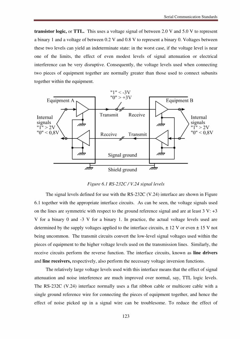
Serial Communication Standards
123
transistor logic, or TTL. This uses a voltage signal of between 2.0 V and 5.0 V to represent
a binary 1 and a voltage of between 0.2 V and 0.8 V to represent a binary 0. Voltages between
these two levels can yield an indeterminate state: in the worst case, if the voltage level is near
one of the limits, the effect of even modest levels of signal attenuation or electrical
interference can be very disruptive. Consequently, the voltage levels used when connecting
two pieces of equipment together are normally greater than those used to connect subunits
together within the equipment.
Figure 6.1 RS-232C / V.24 signal levels
The signal levels defined for use with the RS-232C (V.24) interface are shown in Figure
6.1 together with the appropriate interface circuits. As can be seen, the voltage signals used
on the lines are symmetric with respect to the ground reference signal and are at least 3 V: +3
V for a binary 0 and -3 V for a binary 1. In practice, the actual voltage levels used are
determined by the supply voltages applied to the interface circuits, ± 12 V or even ± 15 V not
being uncommon. The transmit circuits convert the low-level signal voltages used within the
pieces of equipment to the higher voltage levels used on the transmission lines. Similarly, the
receive circuits perform the reverse function. The interface circuits, known as line drivers
and line receivers, respectively, also perform the necessary voltage inversion functions.
The relatively large voltage levels used with this interface means that the effect of signal
attenuation and noise interference are much improved over normal, say, TTL logic levels.
The RS-232C (V.24) interface normally uses a flat ribbon cable or multicore cable with a
single ground reference wire for connecting the pieces of equipment together, and hence the
effect of noise picked up in a signal wire can be troublesome. To reduce the effect of
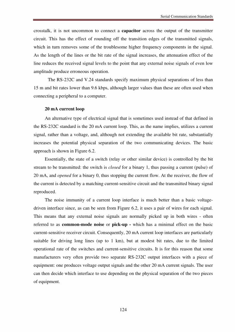
Serial Communication Standards
124
crosstalk, it is not uncommon to connect a capacitor across the output of the transmitter
circuit. This has the effect of rounding off the transition edges of the transmitted signals,
which in turn removes some of the troublesome higher frequency components in the signal.
As the length of the lines or the bit rate of the signal increases, the attenuation effect of the
line reduces the received signal levels to the point that any external noise signals of even low
amplitude produce erroneous operation.
The RS-232C and V.24 standards specify maximum physical separations of less than
15 m and bit rates lower than 9.6 kbps, although larger values than these are often used when
connecting a peripheral to a computer.
20 mA current loop
An alternative type of electrical signal that is sometimes used instead of that defined in
the RS-232C standard is the 20 mA current loop. This, as the name implies, utilizes a current
signal, rather than a voltage, and, although not extending the available bit rate, substantially
increases the potential physical separation of the two communicating devices. The basic
approach is shown in Figure 6.2.
Essentially, the state of a switch (relay or other similar device) is controlled by the bit
stream to be transmitted: the switch is closed for a binary 1, thus passing a current (pulse) of
20 mA, and opened for a binary 0, thus stopping the current flow. At the receiver, the flow of
the current is detected by a matching current-sensitive circuit and the transmitted binary signal
reproduced.
The noise immunity of a current loop interface is much better than a basic voltage-
driven interface since, as can be seen from Figure 6.2, it uses a pair of wires for each signal.
This means that any external noise signals are normally picked up in both wires - often
referred to as common-mode noise or pick-up - which has a minimal effect on the basic
current-sensitive receiver circuit. Consequently, 20 mA current loop interfaces are particularly
suitable for driving long lines (up to 1 km), but at modest bit rates, due to the limited
operational rate of the switches and current-sensitive circuits. It is for this reason that some
manufacturers very often provide two separate RS-232C output interfaces with a piece of
equipment: one produces voltage output signals and the other 20 mA current signals. The user
can then decide which interface to use depending on the physical separation of the two pieces
of equipment.
Serial Communication Standards
125
Figure 6.2 20 mA current loop
6.1.2. RS-422/V.11
If the physical separation and the bit rate are both to be increased, then the alternative
RS-422/V.11 signal definitions should be used. These are based on the use of a twisted pair
cable and a pair of differential (also referred to as double-ended) transmitter and receiver
circuits. A typical circuit arrangement is shown in Figure 6.3.
A differential transmitter circuit produces two signals of equal and opposite polarity for
every binary 1 or 0 signal to be transmitted. As the differential receiver is sensitive only to
the difference between the two signals on its two inputs, any noise picked up in both wires
will not affect the operation of the receiver. Differential receivers, therefore, are said to have
good common-mode rejection properties. A derivative of the RS-422, the RS-423, can be
used to accept the single-ended voltages output by an RS-232C interface with a differential
receiver. The RS-422 is suitable for use with twisted pair cable for physical separations of,
say, 100 m at 1 Mbps or greater distances at lower bit rates.
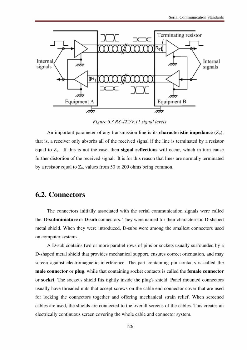
Serial Communication Standards
126
Figure 6.3 RS-422/V.11 signal levels
An important parameter of any transmission line is its characteristic impedance (Zo);
that is, a receiver only absorbs all of the received signal if the line is terminated by a resistor
equal to Zo. If this is not the case, then signal reflections will occur, which in turn cause
further distortion of the received signal. It is for this reason that lines are normally terminated
by a resistor equal to Zo, values from 50 to 200 ohms being common.
6.2. Connectors
The connectors initially associated with the serial communication signals were called
the D-subminiature or D-sub connectors. They were named for their characteristic D-shaped
metal shield. When they were introduced, D-subs were among the smallest connectors used
on computer systems.
A D-sub contains two or more parallel rows of pins or sockets usually surrounded by a
D-shaped metal shield that provides mechanical support, ensures correct orientation, and may
screen against electromagnetic interference. The part containing pin contacts is called the
male connector or plug, while that containing socket contacts is called the female connector
or socket. The socket's shield fits tightly inside the plug's shield. Panel mounted connectors
usually have threaded nuts that accept screws on the cable end connector cover that are used
for locking the connectors together and offering mechanical strain relief. When screened
cables are used, the shields are connected to the overall screens of the cables. This creates an
electrically continuous screen covering the whole cable and connector system.
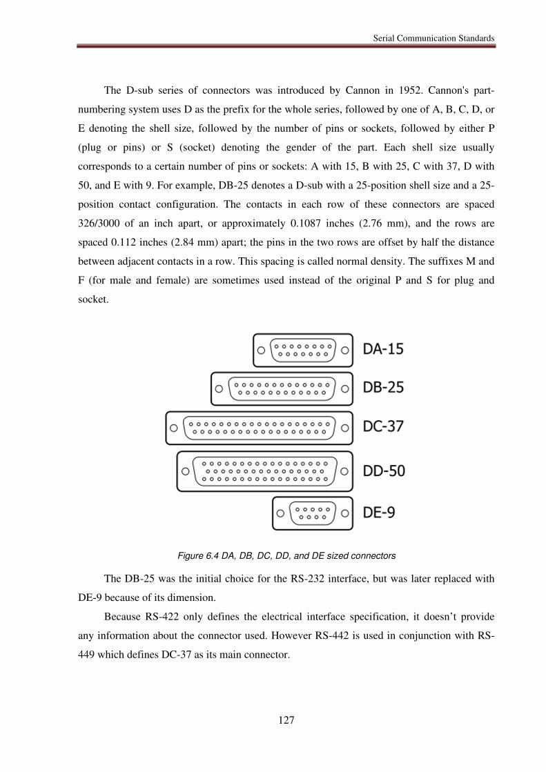
Serial Communication Standards
127
The D-sub series of connectors was introduced by Cannon in 1952. Cannon's part-
numbering system uses D as the prefix for the whole series, followed by one of A, B, C, D, or
E denoting the shell size, followed by the number of pins or sockets, followed by either P
(plug or pins) or S (socket) denoting the gender of the part. Each shell size usually
corresponds to a certain number of pins or sockets: A with 15, B with 25, C with 37, D with
50, and E with 9. For example, DB-25 denotes a D-sub with a 25-position shell size and a 25-
position contact configuration. The contacts in each row of these connectors are spaced
326/3000 of an inch apart, or approximately 0.1087 inches (2.76 mm), and the rows are
spaced 0.112 inches (2.84 mm) apart; the pins in the two rows are offset by half the distance
between adjacent contacts in a row. This spacing is called normal density. The suffixes M and
F (for male and female) are sometimes used instead of the original P and S for plug and
socket.
Figure 6.4 DA, DB, DC, DD, and DE sized connectors
The DB-25 was the initial choice for the RS-232 interface, but was later replaced with
DE-9 because of its dimension.
Because RS-422 only defines the electrical interface specification, it doesn’t provide
any information about the connector used. However RS-442 is used in conjunction with RS-
449 which defines DC-37 as its main connector.
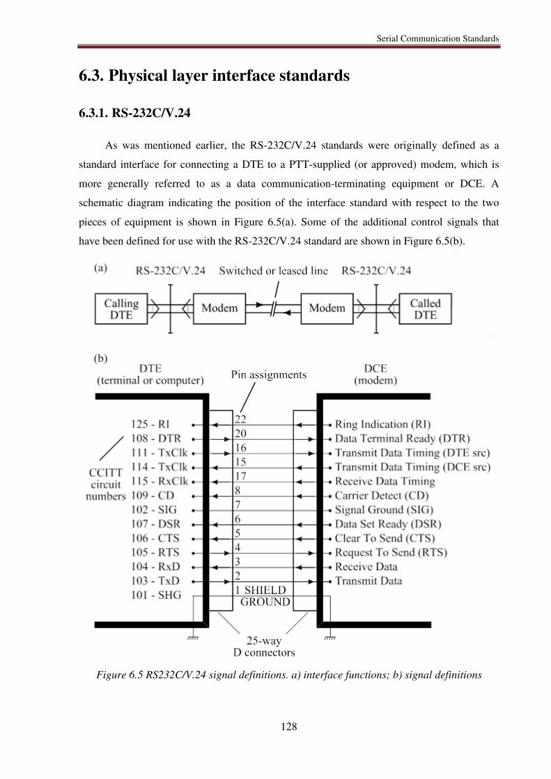
Serial Communication Standards
128
6.3. Physical layer interface standards
6.3.1. RS-232C/V.24
As was mentioned earlier, the RS-232C/V.24 standards were originally defined as a
standard interface for connecting a DTE to a PTT-supplied (or approved) modem, which is
more generally referred to as a data communication-terminating equipment or DCE. A
schematic diagram indicating the position of the interface standard with respect to the two
pieces of equipment is shown in Figure 6.5(a). Some of the additional control signals that
have been defined for use with the RS-232C/V.24 standard are shown in Figure 6.5(b).
Figure 6.5 RS232C/V.24 signal definitions. a) interface functions; b) signal definitions
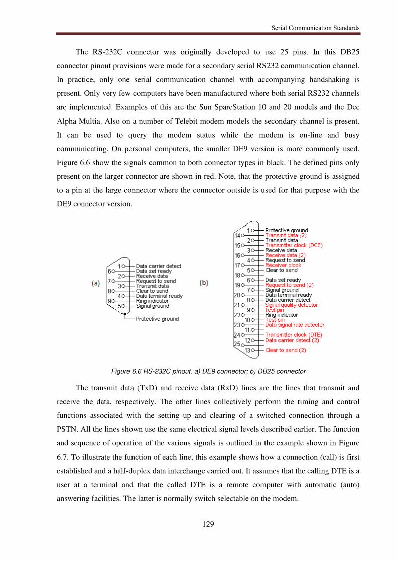
Serial Communication Standards
129
The RS-232C connector was originally developed to use 25 pins. In this DB25
connector pinout provisions were made for a secondary serial RS232 communication channel.
In practice, only one serial communication channel with accompanying handshaking is
present. Only very few computers have been manufactured where both serial RS232 channels
are implemented. Examples of this are the Sun SparcStation 10 and 20 models and the Dec
Alpha Multia. Also on a number of Telebit modem models the secondary channel is present.
It can be used to query the modem status while the modem is on-line and busy
communicating. On personal computers, the smaller DE9 version is more commonly used.
Figure 6.6 show the signals common to both connector types in black. The defined pins only
present on the larger connector are shown in red. Note, that the protective ground is assigned
to a pin at the large connector where the connector outside is used for that purpose with the
DE9 connector version.
Figure 6.6 RS-232C pinout. a) DE9 connector; b) DB25 connector
The transmit data (TxD) and receive data (RxD) lines are the lines that transmit and
receive the data, respectively. The other lines collectively perform the timing and control
functions associated with the setting up and clearing of a switched connection through a
PSTN. All the lines shown use the same electrical signal levels described earlier. The function
and sequence of operation of the various signals is outlined in the example shown in Figure
6.7. To illustrate the function of each line, this example shows how a connection (call) is first
established and a half-duplex data interchange carried out. It assumes that the calling DTE is a
user at a terminal and that the called DTE is a remote computer with automatic (auto)
answering facilities. The latter is normally switch selectable on the modem.
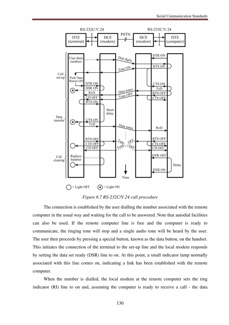
Serial Communication Standards
130
Figure 6.7 RS-232C/V.24 call procedure
The connection is established by the user dialling the number associated with the remote
computer in the usual way and waiting for the call to be answered. Note that autodial facilities
can also be used. If the remote computer line is free and the computer is ready to
communicate, the ringing tone will stop and a single audio tone will be heard by the user.
The user then proceeds by pressing a special button, known as the data button, on the handset.
This initiates the connection of the terminal to the set-up line and the local modem responds
by setting the data set ready (DSR) line to on. At this point, a small indicator lamp normally
associated with this line comes on, indicating a link has been established with the remote
computer.
When the number is dialled, the local modem at the remote computer sets the ring
indicator (RI) line to on and, assuming the computer is ready to receive a call - the data
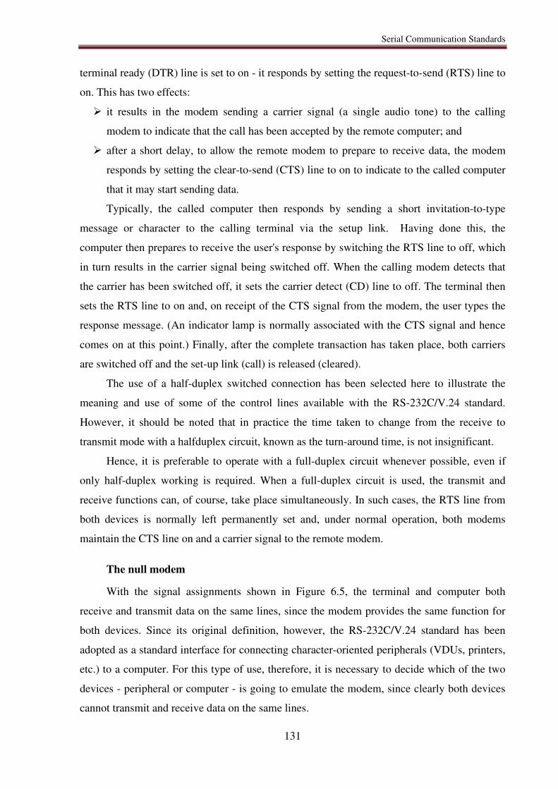
Serial Communication Standards
131
terminal ready (DTR) line is set to on - it responds by setting the request-to-send (RTS) line to
on. This has two effects:
it results in the modem sending a carrier signal (a single audio tone) to the calling
modem to indicate that the call has been accepted by the remote computer; and
after a short delay, to allow the remote modem to prepare to receive data, the modem
responds by setting the clear-to-send (CTS) line to on to indicate to the called computer
that it may start sending data.
Typically, the called computer then responds by sending a short invitation-to-type
message or character to the calling terminal via the setup link. Having done this, the
computer then prepares to receive the user's response by switching the RTS line to off, which
in turn results in the carrier signal being switched off. When the calling modem detects that
the carrier has been switched off, it sets the carrier detect (CD) line to off. The terminal then
sets the RTS line to on and, on receipt of the CTS signal from the modem, the user types the
response message. (An indicator lamp is normally associated with the CTS signal and hence
comes on at this point.) Finally, after the complete transaction has taken place, both carriers
are switched off and the set-up link (call) is released (cleared).
The use of a half-duplex switched connection has been selected here to illustrate the
meaning and use of some of the control lines available with the RS-232C/V.24 standard.
However, it should be noted that in practice the time taken to change from the receive to
transmit mode with a halfduplex circuit, known as the turn-around time, is not insignificant.
Hence, it is preferable to operate with a full-duplex circuit whenever possible, even if
only half-duplex working is required. When a full-duplex circuit is used, the transmit and
receive functions can, of course, take place simultaneously. In such cases, the RTS line from
both devices is normally left permanently set and, under normal operation, both modems
maintain the CTS line on and a carrier signal to the remote modem.
The null modem
With the signal assignments shown in Figure 6.5, the terminal and computer both
receive and transmit data on the same lines, since the modem provides the same function for
both devices. Since its original definition, however, the RS-232C/V.24 standard has been
adopted as a standard interface for connecting character-oriented peripherals (VDUs, printers,
etc.) to a computer. For this type of use, therefore, it is necessary to decide which of the two
devices - peripheral or computer - is going to emulate the modem, since clearly both devices
cannot transmit and receive data on the same lines.
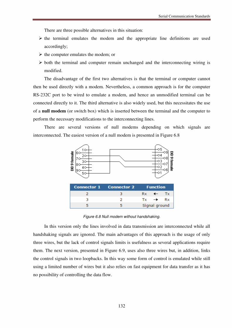
Serial Communication Standards
132
There are three possible alternatives in this situation:
the terminal emulates the modem and the appropriate line definitions are used
accordingly;
the computer emulates the modem; or
both the terminal and computer remain unchanged and the interconnecting wiring is
modified.
The disadvantage of the first two alternatives is that the terminal or computer cannot
then be used directly with a modem. Nevertheless, a common approach is for the computer
RS-232C port to be wired to emulate a modem, and hence an unmodified terminal can be
connected directly to it. The third alternative is also widely used, but this necessitates the use
of a null modem (or switch box) which is inserted between the terminal and the computer to
perform the necessary modifications to the interconnecting lines.
There are several versions of null modems depending on which signals are
interconnected. The easiest version of a null modem is presented in Figure 6.8
Figure 6.8 Null modem without handshaking.
In this version only the lines involved in data transmission are interconnected while all
handshaking signals are ignored. The main advantages of this approach is the usage of only
three wires, but the lack of control signals limits is usefulness as several applications require
them. The next version, presented in Figure 6.9, uses also three wires but, in addition, links
the control signals in two loopbacks. In this way some form of control is emulated while still
using a limited number of wires but it also relies on fast equipment for data transfer as it has
no possibility of controlling the data flow.
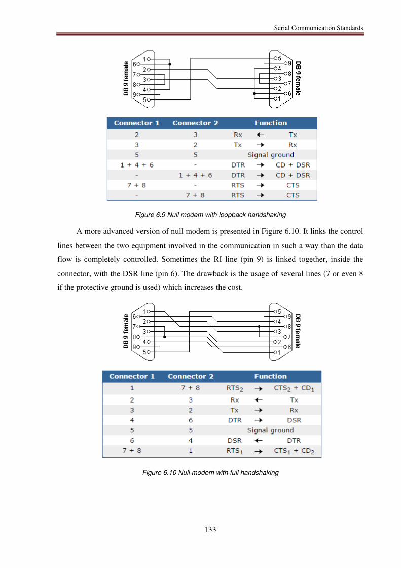
Serial Communication Standards
133
Figure 6.9 Null modem with loopback handshaking
A more advanced version of null modem is presented in Figure 6.10. It links the control
lines between the two equipment involved in the communication in such a way than the data
flow is completely controlled. Sometimes the RI line (pin 9) is linked together, inside the
connector, with the DSR line (pin 6). The drawback is the usage of several lines (7 or even 8
if the protective ground is used) which increases the cost.
Figure 6.10 Null modem with full handshaking
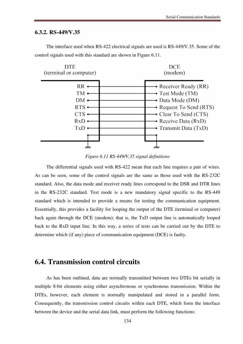
Serial Communication Standards
134
6.3.2. RS-449/V.35
The interface used when RS-422 electrical signals are used is RS-449/V.35. Some of the
control signals used with this standard are shown in Figure 6.11.
Figure 6.11 RS-449/V.35 signal definitions
The differential signals used with RS-422 mean that each line requires a pair of wires.
As can be seen, some of the control signals are the same as those used with the RS-232C
standard. Also, the data mode and receiver ready lines correspond to the DSR and DTR lines
in the RS-232C standard. Test mode is a new mandatory signal specific to the RS-449
standard which is intended to provide a means for testing the communication equipment.
Essentially, this provides a facility for looping the output of the DTE (terminal or computer)
back again through the DCE (modem); that is, the TxD output line is automatically looped
back to the RxD input line. In this way, a series of tests can be carried out by the DTE to
determine which (if any) piece of communication equipment (DCE) is faulty.
6.4. Transmission control circuits
As has been outlined, data are normally transmitted between two DTEs bit serially in
multiple 8-bit elements using either asynchronous or synchronous transmission. Within the
DTEs, however, each element is normally manipulated and stored in a parallel form.
Consequently, the transmission control circuits within each DTE, which form the interface
between the device and the serial data link, must perform the following functions:

Serial Communication Standards
135
parallel-to-serial conversion of each element in preparation for transmission of the
element on the data link;
serial-to-parallel conversion of each received element in preparation for storage and
processing of the element in the device;
a means for the receiver to achieve bit, character and, for synchronous transmission,
frame synchronization;
the generation of suitable error check digits for error-detection purposes and the
detection of such errors should they occur.
To satisfy these requirements, special integrated circuits are now readily available.
Although different circuits can be used to control asynchronous and synchronous data links,
circuits are also available to support both types of link. The latter are often referred to as
Universal Communication Interface Circuits or Universal Synchronous/Asynchronous
Receiver and Transmitter (USART) but, since the two halves of such circuits function
independently, each will be considered separately.
6.4.1. Asynchronous transmission
The interface circuit used to support asynchronous transmission is known as a
Universal Asynchronous Receiver and Transmitter, or simply a UART. It is termed
universal since it is normally a programmable device and the user can, by simply loading a
predefined control word (bit pattern) into the device, specify the required operating
characteristics.
A schematic diagram of a typical UART is shown in Figure 6.12.
To use such a device, the mode (control) register is first loaded with the required bit
pattern to define the required operating characteristics; this is known as initialization.
Typically, the user may select 5, 6, 7 or 8 bits per character, odd, even or zero parity, one or
more stop bits and a range of transmit and receive bit rates. The latter are selected from a
standard range of 50 bps to 19.2 kbps by connecting a clock source of the appropriate
frequency to the transmit and receive clock inputs of the UART and defining the ratio of this
clock to the required bit rate (xl, x16, x32 or x64) in the control word. This clock ratio is used
for bit synchronization (see Chapter Error! Reference source not found., Error! Reference
source not found.).
Figure 6.13(a) illustrates the meaning of the various control bits in a typical device,
the Intel 8251/Signetics 2657. Assuming the bit pattern 01001101 (4D hexadecimal) was
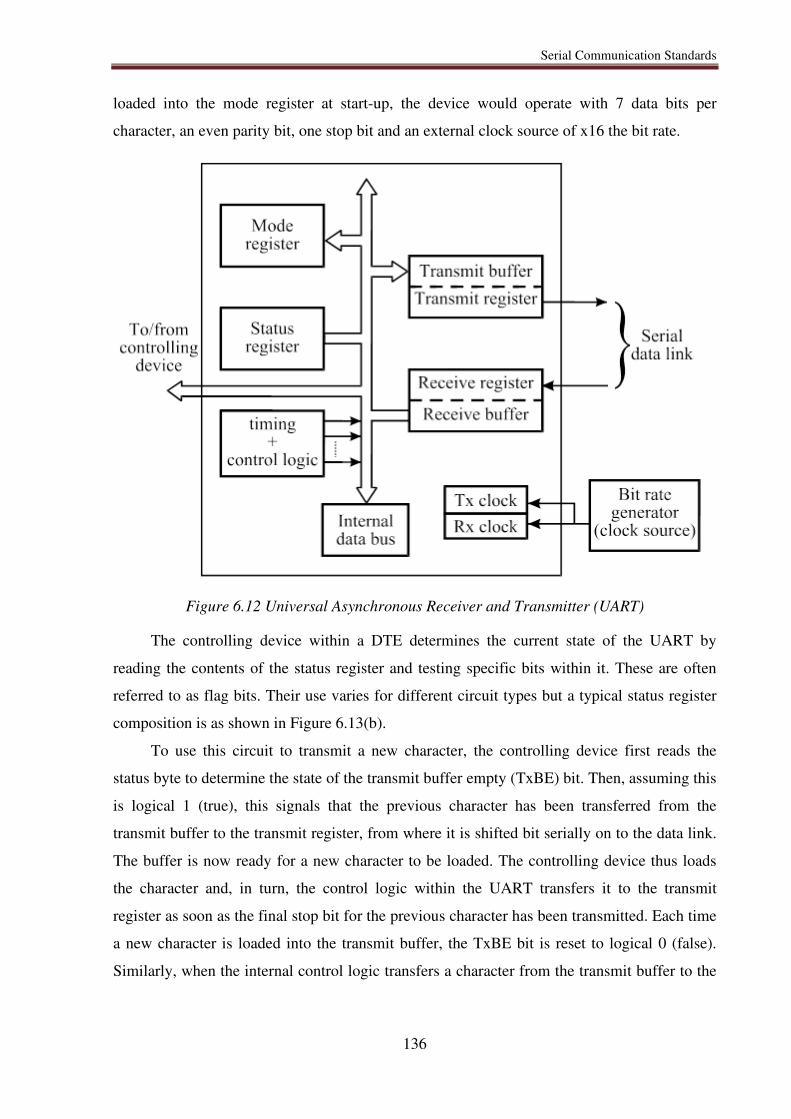
Serial Communication Standards
136
loaded into the mode register at start-up, the device would operate with 7 data bits per
character, an even parity bit, one stop bit and an external clock source of x16 the bit rate.
Figure 6.12 Universal Asynchronous Receiver and Transmitter (UART)
The controlling device within a DTE determines the current state of the UART by
reading the contents of the status register and testing specific bits within it. These are often
referred to as flag bits. Their use varies for different circuit types but a typical status register
composition is as shown in Figure 6.13(b).
To use this circuit to transmit a new character, the controlling device first reads the
status byte to determine the state of the transmit buffer empty (TxBE) bit. Then, assuming this
is logical 1 (true), this signals that the previous character has been transferred from the
transmit buffer to the transmit register, from where it is shifted bit serially on to the data link.
The buffer is now ready for a new character to be loaded. The controlling device thus loads
the character and, in turn, the control logic within the UART transfers it to the transmit
register as soon as the final stop bit for the previous character has been transmitted. Each time
a new character is loaded into the transmit buffer, the TxBE bit is reset to logical 0 (false).
Similarly, when the internal control logic transfers a character from the transmit buffer to the
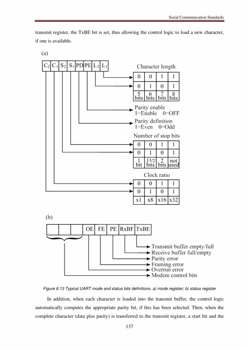
Serial Communication Standards
137
transmit register, the TxBE bit is set, thus allowing the control logic to load a new character,
if one is available.
Figure 6.13 Typical UART mode and status bits definitions. a) mode register; b) status register
In addition, when each character is loaded into the transmit buffer, the control logic
automatically computes the appropriate parity bit, if this has been selected. Then, when the
complete character (data plus parity) is transferred to the transmit register, a start bit and the
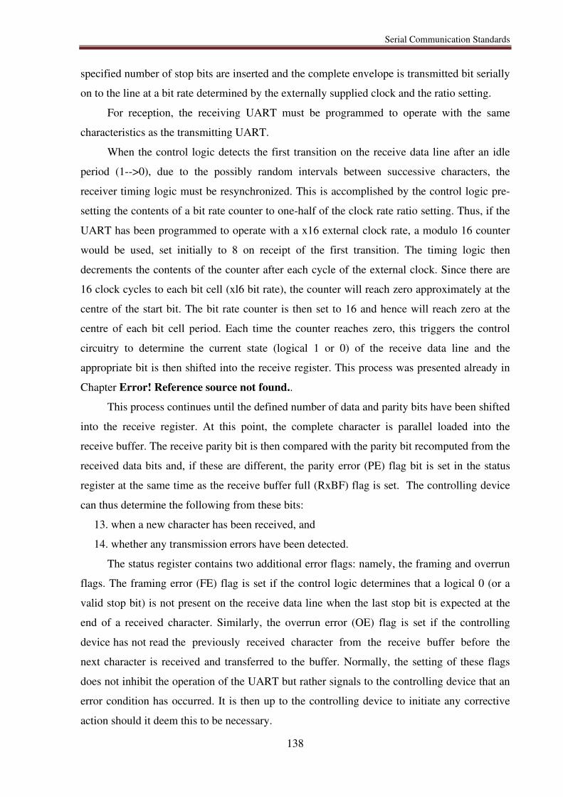
Serial Communication Standards
138
specified number of stop bits are inserted and the complete envelope is transmitted bit serially
on to the line at a bit rate determined by the externally supplied clock and the ratio setting.
For reception, the receiving UART must be programmed to operate with the same
characteristics as the transmitting UART.
When the control logic detects the first transition on the receive data line after an idle
period (1-->0), due to the possibly random intervals between successive characters, the
receiver timing logic must be resynchronized. This is accomplished by the control logic pre-
setting the contents of a bit rate counter to one-half of the clock rate ratio setting. Thus, if the
UART has been programmed to operate with a x16 external clock rate, a modulo 16 counter
would be used, set initially to 8 on receipt of the first transition. The timing logic then
decrements the contents of the counter after each cycle of the external clock. Since there are
16 clock cycles to each bit cell (xl6 bit rate), the counter will reach zero approximately at the
centre of the start bit. The bit rate counter is then set to 16 and hence will reach zero at the
centre of each bit cell period. Each time the counter reaches zero, this triggers the control
circuitry to determine the current state (logical 1 or 0) of the receive data line and the
appropriate bit is then shifted into the receive register. This process was presented already in
Chapter Error! Reference source not found..
This process continues until the defined number of data and parity bits have been shifted
into the receive register. At this point, the complete character is parallel loaded into the
receive buffer. The receive parity bit is then compared with the parity bit recomputed from the
received data bits and, if these are different, the parity error (PE) flag bit is set in the status
register at the same time as the receive buffer full (RxBF) flag is set. The controlling device
can thus determine the following from these bits:
13. when a new character has been received, and
14. whether any transmission errors have been detected.
The status register contains two additional error flags: namely, the framing and overrun
flags. The framing error (FE) flag is set if the control logic determines that a logical 0 (or a
valid stop bit) is not present on the receive data line when the last stop bit is expected at the
end of a received character. Similarly, the overrun error (OE) flag is set if the controlling
device has not read the previously received character from the receive buffer before the
next character is received and transferred to the buffer. Normally, the setting of these flags
does not inhibit the operation of the UART but rather signals to the controlling device that an
error condition has occurred. It is then up to the controlling device to initiate any corrective
action should it deem this to be necessary.
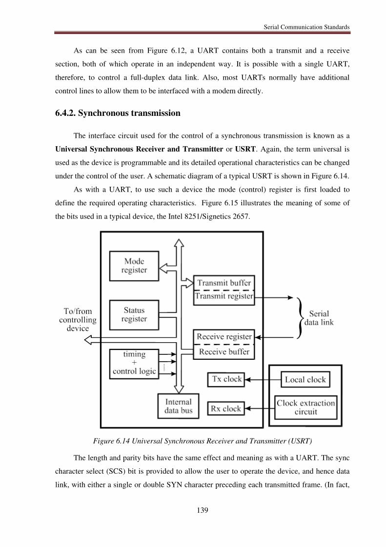
Serial Communication Standards
139
As can be seen from Figure 6.12, a UART contains both a transmit and a receive
section, both of which operate in an independent way. It is possible with a single UART,
therefore, to control a full-duplex data link. Also, most UARTs normally have additional
control lines to allow them to be interfaced with a modem directly.
6.4.2. Synchronous transmission
The interface circuit used for the control of a synchronous transmission is known as a
Universal Synchronous Receiver and Transmitter or USRT. Again, the term universal is
used as the device is programmable and its detailed operational characteristics can be changed
under the control of the user. A schematic diagram of a typical USRT is shown in Figure 6.14.
As with a UART, to use such a device the mode (control) register is first loaded to
define the required operating characteristics. Figure 6.15 illustrates the meaning of some of
the bits used in a typical device, the Intel 8251/Signetics 2657.
Figure 6.14 Universal Synchronous Receiver and Transmitter (USRT)
The length and parity bits have the same effect and meaning as with a UART. The sync
character select (SCS) bit is provided to allow the user to operate the device, and hence data
link, with either a single or double SYN character preceding each transmitted frame. (In fact,

Serial Communication Standards
140
the actual sync character used can normally be selected at start-up also.) The controlling
device determines the current state of the USRT by reading the contents of the status register
and testing specific bits within it for example, the TxBE bit, the RxBF bit, etc.
At the start of transmission, the controlling device initiates the transmission of several
SYN characters to allow the receiving device to achieve character synchronism. This is
achieved by loading SYN characters into the transmit buffer each time the TxBE bit becomes
set (logical 1). The contents of the frame to be transmitted are then transferred by the
controlling device to the transmit buffer a single character at a time, the rate again being
controlled by the state of the TxBE bit. After the last character of the frame has been
transmitted, the USRT automatically starts to transmit SYN characters until the controlling
device is ready to transmit a new frame. These are referred to as inter-frame time-fill
characters and they allow the receiver to maintain character synchronism between successive
frames.
Figure 6.15 Typical USRT mode and status bits definitions. a) mode register; b) status register
At the destination, the controlling device first sets the receiving USRT into hunt mode,
which causes the control logic to compare the contents of the receive buffer with the SYN
character, after each new bit is received. When a match is found, the sync detect (SYNDET)
bit in the status register is set to indicate to the controlling device that character synchronism
has been obtained. The latter then waits for the start-of-frame character (STX) to indicate that
a new frame is being received. Each character of the frame is then received by the controlling
device, under the control of the RxBF bit, until the end-of-frame character (ETX) is detected.
In the synchronous mode, all data are transmitted and received at a rate determined by the
Serial Communication Standards
141
transmit and receive clocks, respectively. The latter is normally derived from the incoming bit
stream using a suitable clock extraction circuit.
The circuits available for the control of a bit-oriented line normally contain features that
perform frame synchronization and zero bit insertion and deletion. In addition, as for a
character-oriented USRT, they also include features for such functions as the generation and
detection of transmission errors.
Universal Serial Bus
142
7. Universal Serial Bus
7.1. History
A group of seven companies began the development of USB in 1994: Compaq, DEC,
IBM, Intel, Microsoft, NEC, and Nortel. The goal was to make it fundamentally easier to
connect external devices to PCs by replacing the multitude of connectors at the back of PCs,
addressing the usability issues of existing interfaces, and simplifying software configuration
of all devices connected to USB, as well as permitting greater data rates for external devices.
A team including Ajay Bhatt worked on the standard at Intel the first integrated circuits
supporting USB were produced by Intel in 1995.
Released in January 1996, USB 1.0 specified data rates of 1.5 Mbit/s (Low Bandwidth
or Low Speed) and 12 Mbit/s (Full Bandwidth or Full Speed). It did not allow for extension
cables or pass-through monitors, due to timing and power limitations. Few USB devices made
it to the market until USB 1.1 was released in August 1998, fixing problems identified in 1.0,
mostly related to using hubs. USB 1.1 was the earliest revision that was widely adopted.
Apple Inc.'s iMac was the first mainstream usage of USB and the iMac's success popularized
USB itself. Following Apple's design decision to remove all legacy ports from the iMac,
many PC manufactures began building legacy-free PCs, which lead to the broader PC market
using USB as a standard.
The USB 2.0 specification was released in April 2000 and was ratified by the USB
Implementers Forum (USB-IF) at the end of 2001. Hewlett-Packard, Intel, Lucent
Technologies (now Alcatel-Lucent), NEC, and Philips jointly led the initiative to develop a
higher data transfer rate, with the resulting specification achieving 480 Mbit/s (High Speed),
a 40-times increase over the original USB 1.1 specification. Due to bus access constraints, the
effective throughput of the High Speed signaling rate is limited to 35 MB/s or 280 Mbit/s.
The USB 3.0 specification was published on 12 November 2008. Its main goals were to
increase the data transfer rate (up to 5 Gbit/s), decrease power consumption, increase power
output, and be backward compatible with USB 2.0. USB 3.0 includes a new, higher speed bus

Universal Serial Bus
143
called SuperSpeed in parallel with the USB 2.0 bus. The payload throughput is 4 Gbit/s (due
to the overhead incurred by 8b/10b encoding), and the specification considers it reasonable to
achieve around 3.2 Gbit/s (0.4 GB/s or 400 MB/s), which should increase with future
hardware advances. Communication is full-duplex in SuperSpeed transfer mode; in the modes
supported previously, by 1.x and 2.0, communication is half-duplex, with direction controlled
by the host.
A January 2013 press release from the USB group revealed plans to update USB 3.0 to
10 Gbit/s. The group ended up creating a new USB version, USB 3.1, which was released on
31 July 2013, introducing a faster transfer mode called SuperSpeed USB 10 Gbit/s (or
SuperSpeedPlus), putting it on par with a single first-generation Thunderbolt channel. The
USB 3.1 standard is backward compatible with USB 3.0 and USB 2.0.
For marketing purpose the 5Gbit/s USB 3.0 was renamed USB 3.1 Gen1, while the
10Gbit/s USB 3.1 was renamed USB 3.1 Gen2.
7.2. Architectural Overview
7.2.1. Bus components
USB communications require a host computer with USB support, a device with a USB
port, and hubs, connectors, and cables as needed to connect the device to the host computer.
The host computer is a PC or a handheld device or other embedded system that contains
USB host-controller hardware and a root hub. The host controller formats data for
transmitting on the bus and translates received data to a format that operating-system
components understand. The host controller also helps manage communications on the bus.
The root hub has one or more connectors for attaching devices. The root hub and host
controller together detect device attachment and removal, carry out requests from the host
controller, and pass data between devices and the host controller. In addition to the root hub, a
bus may have one or more external hubs.
7.2.2. Topology
The topology, or arrangement of connections, on the bus is a tiered star (Figure 7.1).
At the center of each star is a hub, and each connection to the hub is a point on the star. The
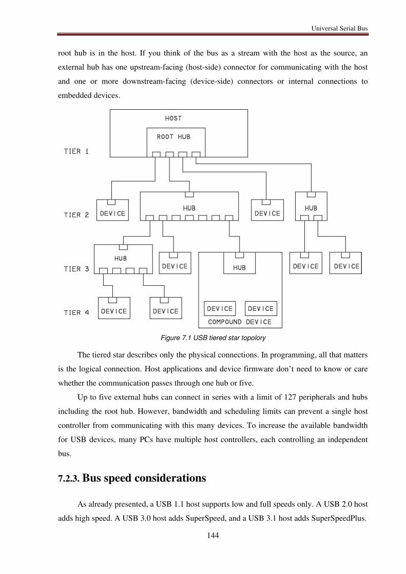
Universal Serial Bus
144
root hub is in the host. If you think of the bus as a stream with the host as the source, an
external hub has one upstream-facing (host-side) connector for communicating with the host
and one or more downstream-facing (device-side) connectors or internal connections to
embedded devices.
Figure 7.1 USB tiered star topolory
The tiered star describes only the physical connections. In programming, all that matters
is the logical connection. Host applications and device firmware don’t need to know or care
whether the communication passes through one hub or five.
Up to five external hubs can connect in series with a limit of 127 peripherals and hubs
including the root hub. However, bandwidth and scheduling limits can prevent a single host
controller from communicating with this many devices. To increase the available bandwidth
for USB devices, many PCs have multiple host controllers, each controlling an independent
bus.
7.2.3. Bus speed considerations
As already presented, a USB 1.1 host supports low and full speeds only. A USB 2.0 host
adds high speed. A USB 3.0 host adds SuperSpeed, and a USB 3.1 host adds SuperSpeedPlus.
Universal Serial Bus
145
A USB 3.1 hub contains both a USB 2.0 hub and a SuperSpeed/SuperSpeedPlus hub.
The hub handles traffic at any speed. SuperSpeed and SuperSpeedPlus traffic uses the
SuperSpeed/SuperSpeedPlus hub’s circuits and wires, and other traffic uses the USB 2.0
hub’s circuits and wires. A USB 3.0 hub is similar but doesn’t support SuperSpeedPlus.
A SuperSpeed-capable device communicates at SuperSpeed only if the host and all hubs
between the host and device are USB 3.1 hubs (Figure 7.2). Otherwise the device must use a
slower speed. In a similar way, a SuperSpeedPlus-capable device communicates at
SuperSpeedPlus only if the host and all hubs between the host and device are USB 3.1 hubs.
On a USB 3.0 bus or with a USB 3.0 hub, a SuperSpeedPlus device communicates at
SuperSpeed.
Figure 7.2 USB 3.1 hosts and hubs support all five speeds for downstream communications.
For compatibility with USB 2.0 hosts and hubs, a SuperSpeed or SuperSpeedPlus
device that doesn’t fully function at a USB 2.0 speed must at least respond to bus resets and
Universal Serial Bus
146
standard requests at a USB 2.0 speed so the device can inform the host that the device
requires a higher speed to perform its function.
A USB 2.0 high-speed-capable device communicates at high speed if the host and all
hubs between are USB 2.0 or USB 3.1 hubs (Figure 7.3). For compatibility with USB 1.1
hosts and hubs, a high-speed device that doesn’t fully function at full speed must at least
respond to bus resets and standard requests at full speed so the device can inform the host that
the device requires high speed to perform its function. Many high-speed devices function,
though more slowly, at full speed because adding support for full speed is generally easy and
is required to pass USB-IF compliance tests.
Figure 7.3 USB 2.0 hubs use high speed for upstream communications if the host and all hubs between are USB 2.0 or higher.
A device that supports full or low speed communicates with its nearest hub at the
supported speed. For any segments upstream from that hub, if all upstream hubs are USB 2.0
or higher, the device’s traffic travels at high speed.
7.2.4. Terminology
In the world of USB, the words function and device have specific meanings. Also
important is the concept of a USB port and how it differs from other ports such as RS-232.
Universal Serial Bus
147
Function
A USB function is a set of one or more related interfaces that expose a capability.
Examples of functions are a mouse, a set of speakers, a data-acquisition unit, or a hub. A
single physical device can contain multiple functions. For example, a device might provide
both printer and scanner functions. A host identifies a device’s functions by requesting a
device descriptor and one or more interface descriptors from the device. The descriptors are
data structures that contain information about the device.
Device
A device is a logical or physical entity that performs one or more functions. Hubs and
peripherals are devices. The host assigns a unique address to each device on the bus. A
compound device contains a hub with one or more permanently attached devices. The host
treats a compound device in much the same way as if the hub and its functions were separate
physical devices. The hub and embedded devices each have a unique address.
A USB 3.1 hub is a special case. The hub contains both a USB 2.0 hub function and a
USB 3.1 hub function.
A composite device has one bus address but multiple, independent interfaces or groups
of related interfaces that each provide a function. Each interface or group of related interfaces
can use a different driver on the host. For example, a composite device could have interfaces
for a printer and a drive. Composite devices are very common.
7.3. Division of labor
The host and its devices each have defined responsibilities. The host bears most of the
burden of managing communications, but a device must have the intelligence to respond to
communications from the host and other events on the bus.
7.3.1. Host responsibilities
To communicate with USB devices, a computer needs hardware and software that
support the USB host function. The hardware consists of a USB host controller and a root hub
with one or more USB ports. The software support is typically an operating system that
Universal Serial Bus
148
enables device drivers to communicate with lower-level drivers that access the USB
hardware.
PCs have one or more hardware host controllers that each support multiple ports. The
host is in charge of the bus. The host has to know what devices are on the bus and the
capabilities of each device. The host must also do its best to ensure that all devices on the bus
can send and receive data as needed. A bus may have many devices, each with different
requirements, all wanting to transfer data at the same time. The host’s job isn’t trivial.
Fortunately, the host-controller hardware and drivers in Windows and other OSes do
much of the work of managing the bus. Each device attached to the host must have an
assigned device driver that enables applications to communicate with the device. System-level
software components manage communications between the device driver and the host
controller and root hub.
Applications don’t have to know the hardware-specific details of communicating with
devices. All the application has to do is send and receive data using standard operating-system
functions or other software components. Often the application doesn’t have to know or care
whether the device uses USB or another interface.
The host must detect devices, manage data flow, perform error checking, provide and
manage power, and exchange data with devices.
Detect devices
On power up, hubs make the host aware of all attached USB devices. In a process called
enumeration, the host determines what bus speed to use, assigns an address, and requests
additional information. After power up, whenever a device is removed or attached, a hub
informs the host of the event, and the host enumerates any newly attached device and removes
any detached device from its list of devices available to applications.
Manage data flow
The host manages traffic on the bus. Multiple devices may want to transfer data at the
same time. The host controller divides the available time into intervals and gives each
transmission a portion of the available time. A USB 2.0 host can send or receive data at one
USB 2.0 speed at a time. A USB 3.1 host can simultaneously transmit SuperSpeed or
SuperSpeedPlus data, receive SuperSpeed or SuperSpeedPlus data, and send or receive data at
a USB 2.0 speed.
Universal Serial Bus
149
During enumeration, a device’s driver requests bandwidth for any transfer types that
must have guaranteed timing. If the bandwidth isn’t available, the driver can request a smaller
portion of the bandwidth or wait until the requested bandwidth is available. Transfers that
have no guaranteed timing use the remaining bandwidth and must wait if the bus is busy with
higher priority data.
Error checking
When transferring data, the host adds error-checking bits. On receiving data, the device
performs calculations on the data and compares the result with received error-checking bits. If
the results don’t match, the device doesn’t acknowledge receiving the data and the host knows
it should retransmit. In a similar way, the host error-checks data received from devices. USB
also supports a transfer type without acknowledgments for use with data such as real-time
audio, which can tolerate occasional errors but needs a constant transfer rate.
If a transmission attempt fails after multiple tries, the host can inform the device’s
driver of the problem, and the driver can notify the application so it can take action as needed.
Provide and manage power
In addition to data wires, a USB cable has wires for a power supply and ground. The
default power is a nominal +5 V. The host provides power to all devices on power up or
attachment and works with the devices to conserve power when possible. Some devices draw
all of their power from the bus.
A high-power USB 2.0 device can draw up to 500 mA from the bus. A high-power
SuperSpeed or SuperSpeedPlus device can draw up to 900 mA from an Enhanced SuperSpeed
bus. Ports on some battery-powered hosts and hubs support only low-power devices, which
are limited to 100 mA (USB 2.0) or 150 mA (Enhanced SuperSpeed). To conserve power
when the bus is idle, a host can require devices to enter a low-power state and reduce their use
of bus current.
Hosts and devices that support USB Power Delivery Rev. 2.0, v1.0 can negotiate for bus
currents up to 5 A and voltages up to 20 V.
Exchange data with devices
All of the above tasks support the host’s main job, which is to exchange data with
devices. In some cases, a device driver requests the host to attempt to send or receive data at
Universal Serial Bus
150
defined intervals, while in others the host communicates only when an application or other
software component requests a transfer.
7.3.2. Device responsibilities
In many ways, a device’s responsibilities are a mirror image of the host’s. When the
host initiates communications, the device must respond. But devices also have duties that are
unique. The device-controller hardware typically handles much of the load. The amount of
needed firmware support varies with the chip architecture. Devices must detect
communications directed to the device, respond to standard requests, perform error checking,
manage power, and exchange data with the host.
Detect communications
Devices must detect communications directed to the device’s address on the bus. The
device stores received data in a buffer and returns a status code or sends requested data or a
status code. In almost all controllers, these functions are built into the hardware and require no
support in code besides preparing the buffers to send or receive data. The firmware doesn’t
have to take other action or make decisions until the chip has detected a communication
intended for the device’s address. Enhanced SuperSpeed devices have less of a burden in
detecting communications because the host routes Enhanced SuperSpeed communications
only to the target device.
Respond to standard requests
On power up or when a device attaches to a powered system, a device must respond to
standard requests sent by the host computer during enumeration and after enumeration
completes.
All devices must respond to these requests, which query the capabilities and status of
the device or request the device to take other action. On receiving a request, the device places
data or status information in a buffer to send to the host. For some requests, such as selecting
a configuration, the device takes other action in addition to responding to the host computer.
The USB specification defines requests, and a class or vendor may define additional
requests. On receiving a request the device doesn’t support, the device responds with a status
code.
Universal Serial Bus
151
Error check
Like the host, a device adds error-checking bits to the data it sends. On receiving data
that includes error-checking bits, the device performs the error-checking calculations. The
device’s response or lack of response tells the host whether to retransmit. The device also
detects the acknowledgment the host returns on receiving data from the device. The device
controller’s hardware typically performs these functions.
Manage power
A device may have its own power supply, obtain power from the bus, or use power from
both sources. A host can request a device to enter the low-power Suspend state, which
requires the device to draw no more than 2.5 mA of bus current. Some devices support remote
wakeup, which can request to exit the Suspend state. USB 3.1 hosts can place individual
functions within a USB 3.1 device in the Suspend state. With host support, devices can use
additional, less restrictive low-power states to conserve power and extend battery life.
Exchange data with the host
All of the above tasks support the main job of a device’s USB port, which is to
exchange data with the host computer. For most transfers where the host sends data to the
device, the device responds to each transfer attempt by sending a code that indicates whether
the device accepted the data or was too busy to accept it. For most transfers where the device
sends data to the host, the device must respond to each attempt by returning data or a code
indicating the device has no data to send. Typically, the hardware responds according to
firmware settings and the error-checking result. Some transfer types don’t use
acknowledgments, and the sender receives no feedback about whether the receiver accepted
transmitted data.
Devices send data only at the host’s request. Enhanced SuperSpeed devices can send a
packet that causes the host to request data from the device.
The controller chip’s hardware handles the details of formatting the data for the bus.
The formatting includes adding error-checking bits to data to transmit, checking for errors in
received data, and sending and receiving the individual bits on the bus.
Of course, the device must also do whatever other tasks it’s responsible for. For
example, a mouse must be ready to detect movement and button clicks and a printer must use
received data to generate printouts.

Universal Serial Bus
152
7.4. Connectors
The connectors the USB committee specifies support a number of USB's underlying
goals, and reflect lessons learned from the many connectors the computer industry has used.
The connector mounted on the host or device is called the receptacle, and the connector
attached to the cable is called the plug. The official USB specification documents also
periodically define the term male to represent the plug, and female to represent the receptacle.
By design, it is difficult to insert a USB plug into its receptacle incorrectly. The USB
specification states that the required USB icon must be embossed on the "topside" of the USB
plug, which "...provides easy user recognition and facilitates alignment during the mating
process." The specification also shows that the "recommended" "Manufacturer's logo" is on
the opposite side of the USB icon. The specification further states, "The USB Icon is also
located adjacent to each receptacle. Receptacles should be oriented to allow the icon on the
plug to be visible during the mating process." However, the specification does not consider
the height of the device compared to the eye level height of the user, so the side of the cable
that is "visible" when mated to a computer on a desk can depend on whether the user is
standing or kneeling.
Only moderate force is needed to insert or remove a USB cable. USB cables and small
USB devices are held in place by the gripping force from the receptacle (without need of the
screws, clips, or thumb-turns other connectors have required).
There are several types of USB connector, including some that have been added while
the specification progressed. The original USB specification detailed standard-A and
standard-B plugs and receptacles; the B connector was necessary so that cabling could be plug
ended at both ends and still prevent users from connecting one computer receptacle to
another. The first engineering change notice to the USB 2.0 specification added mini-B plugs
and receptacles.
Each connector has four contacts: two for carrying differential data and two for
powering the USB device. The data pins in the standard plugs are actually recessed in the plug
compared to the outside power pins. This permits the power pins to connect first, preventing
data errors by allowing the device to power up first and then establish the data connection.
Also, some devices operate in different modes depending on whether the data connection is
made.
To reliably enable a charge-only feature, modern USB accessory peripherals now
include charging cables that provide power connections to the host port but no data
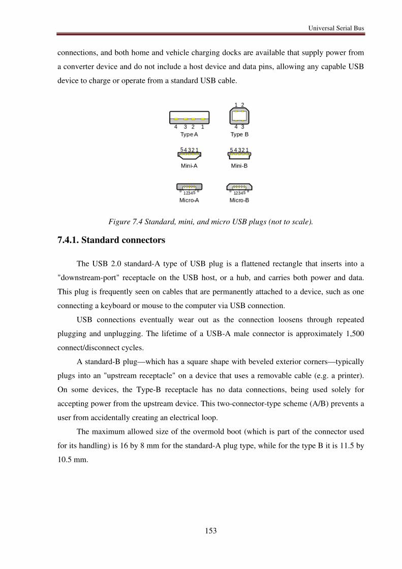
Universal Serial Bus
153
connections, and both home and vehicle charging docks are available that supply power from
a converter device and do not include a host device and data pins, allowing any capable USB
device to charge or operate from a standard USB cable.
Figure 7.4 Standard, mini, and micro USB plugs (not to scale).
7.4.1. Standard connectors
The USB 2.0 standard-A type of USB plug is a flattened rectangle that inserts into a
"downstream-port" receptacle on the USB host, or a hub, and carries both power and data.
This plug is frequently seen on cables that are permanently attached to a device, such as one
connecting a keyboard or mouse to the computer via USB connection.
USB connections eventually wear out as the connection loosens through repeated
plugging and unplugging. The lifetime of a USB-A male connector is approximately 1,500
connect/disconnect cycles.
A standard-B plug—which has a square shape with beveled exterior corners—typically
plugs into an "upstream receptacle" on a device that uses a removable cable (e.g. a printer).
On some devices, the Type-B receptacle has no data connections, being used solely for
accepting power from the upstream device. This two-connector-type scheme (A/B) prevents a
user from accidentally creating an electrical loop.
The maximum allowed size of the overmold boot (which is part of the connector used
for its handling) is 16 by 8 mm for the standard-A plug type, while for the type B it is 11.5 by
10.5 mm.
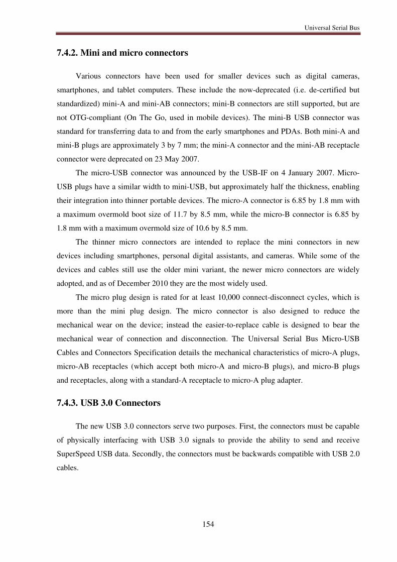
Universal Serial Bus
154
7.4.2. Mini and micro connectors
Various connectors have been used for smaller devices such as digital cameras,
smartphones, and tablet computers. These include the now-deprecated (i.e. de-certified but
standardized) mini-A and mini-AB connectors; mini-B connectors are still supported, but are
not OTG-compliant (On The Go, used in mobile devices). The mini-B USB connector was
standard for transferring data to and from the early smartphones and PDAs. Both mini-A and
mini-B plugs are approximately 3 by 7 mm; the mini-A connector and the mini-AB receptacle
connector were deprecated on 23 May 2007.
The micro-USB connector was announced by the USB-IF on 4 January 2007. Micro-
USB plugs have a similar width to mini-USB, but approximately half the thickness, enabling
their integration into thinner portable devices. The micro-A connector is 6.85 by 1.8 mm with
a maximum overmold boot size of 11.7 by 8.5 mm, while the micro-B connector is 6.85 by
1.8 mm with a maximum overmold size of 10.6 by 8.5 mm.
The thinner micro connectors are intended to replace the mini connectors in new
devices including smartphones, personal digital assistants, and cameras. While some of the
devices and cables still use the older mini variant, the newer micro connectors are widely
adopted, and as of December 2010 they are the most widely used.
The micro plug design is rated for at least 10,000 connect-disconnect cycles, which is
more than the mini plug design. The micro connector is also designed to reduce the
mechanical wear on the device; instead the easier-to-replace cable is designed to bear the
mechanical wear of connection and disconnection. The Universal Serial Bus Micro-USB
Cables and Connectors Specification details the mechanical characteristics of micro-A plugs,
micro-AB receptacles (which accept both micro-A and micro-B plugs), and micro-B plugs
and receptacles, along with a standard-A receptacle to micro-A plug adapter.
7.4.3. USB 3.0 Connectors
The new USB 3.0 connectors serve two purposes. First, the connectors must be capable
of physically interfacing with USB 3.0 signals to provide the ability to send and receive
SuperSpeed USB data. Secondly, the connectors must be backwards compatible with USB 2.0
cables.
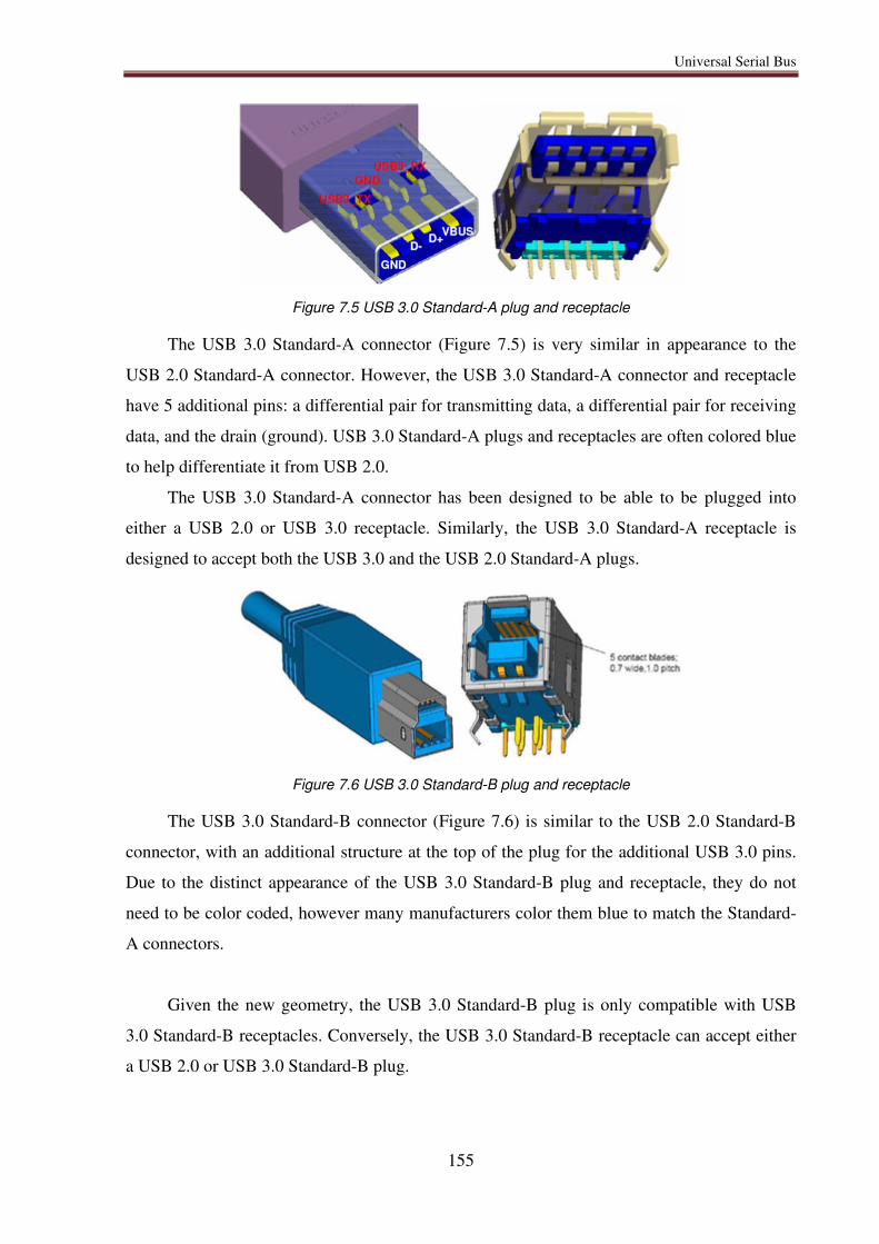
Universal Serial Bus
155
Figure 7.5 USB 3.0 Standard-A plug and receptacle
The USB 3.0 Standard-A connector (Figure 7.5) is very similar in appearance to the
USB 2.0 Standard-A connector. However, the USB 3.0 Standard-A connector and receptacle
have 5 additional pins: a differential pair for transmitting data, a differential pair for receiving
data, and the drain (ground). USB 3.0 Standard-A plugs and receptacles are often colored blue
to help differentiate it from USB 2.0.
The USB 3.0 Standard-A connector has been designed to be able to be plugged into
either a USB 2.0 or USB 3.0 receptacle. Similarly, the USB 3.0 Standard-A receptacle is
designed to accept both the USB 3.0 and the USB 2.0 Standard-A plugs.
Figure 7.6 USB 3.0 Standard-B plug and receptacle
The USB 3.0 Standard-B connector (Figure 7.6) is similar to the USB 2.0 Standard-B
connector, with an additional structure at the top of the plug for the additional USB 3.0 pins.
Due to the distinct appearance of the USB 3.0 Standard-B plug and receptacle, they do not
need to be color coded, however many manufacturers color them blue to match the Standard-
A connectors.
Given the new geometry, the USB 3.0 Standard-B plug is only compatible with USB
3.0 Standard-B receptacles. Conversely, the USB 3.0 Standard-B receptacle can accept either
a USB 2.0 or USB 3.0 Standard-B plug.
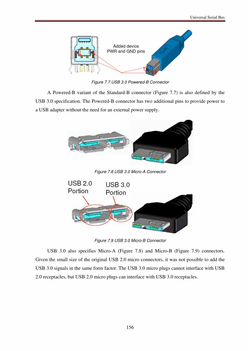
Universal Serial Bus
156
Figure 7.7 USB 3.0 Powered-B Connector
A Powered-B variant of the Standard-B connector (Figure 7.7) is also defined by the
USB 3.0 specification. The Powered-B connector has two additional pins to provide power to
a USB adapter without the need for an external power supply.
Figure 7.8 USB 3.0 Micro-A Connector
Figure 7.9 USB 3.0 Micro-B Connector
USB 3.0 also specifies Micro-A (Figure 7.8) and Micro-B (Figure 7.9) connectors.
Given the small size of the original USB 2.0 micro connectors, it was not possible to add the
USB 3.0 signals in the same form factor. The USB 3.0 micro plugs cannot interface with USB
2.0 receptacles, but USB 2.0 micro plugs can interface with USB 3.0 receptacles.
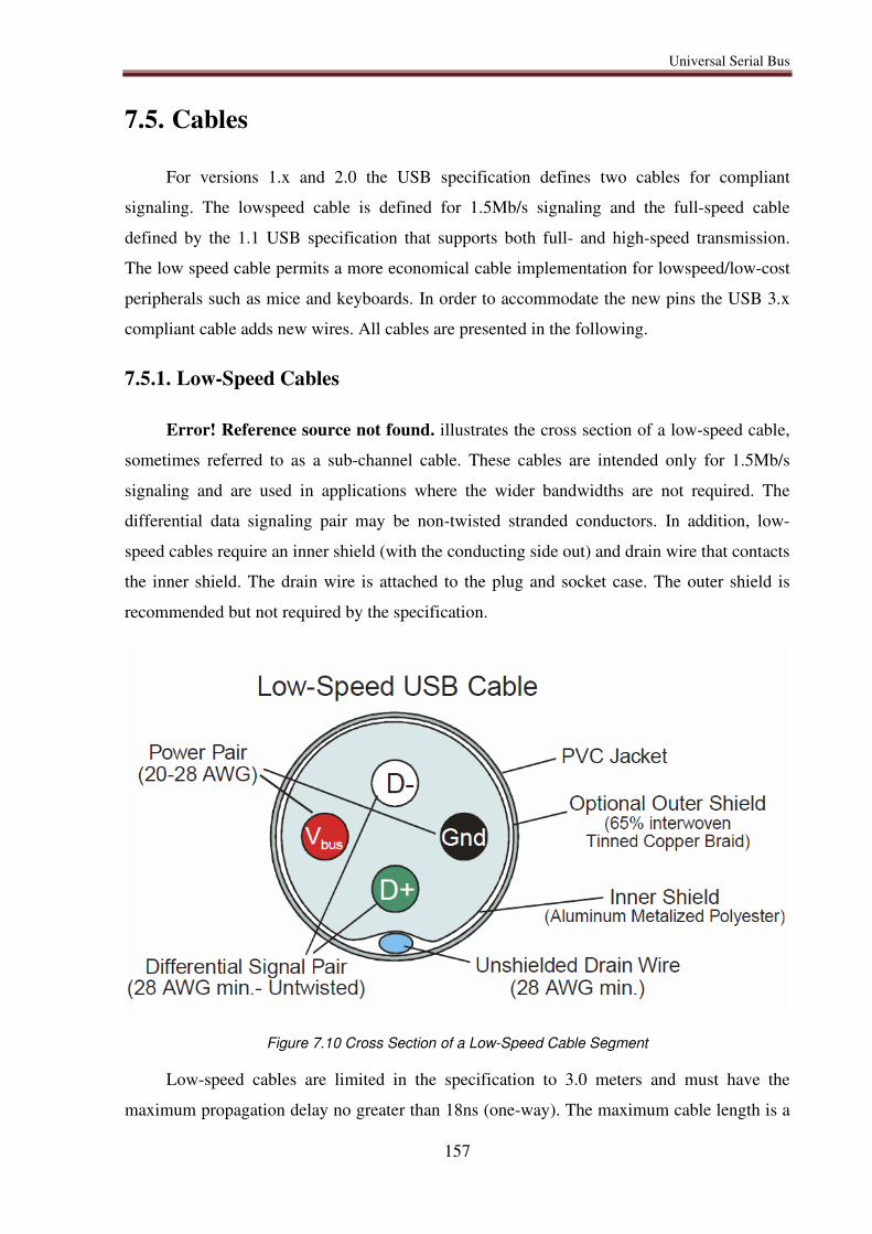
Universal Serial Bus
157
7.5. Cables
For versions 1.x and 2.0 the USB specification defines two cables for compliant
signaling. The lowspeed cable is defined for 1.5Mb/s signaling and the full-speed cable
defined by the 1.1 USB specification that supports both full- and high-speed transmission.
The low speed cable permits a more economical cable implementation for lowspeed/low-cost
peripherals such as mice and keyboards. In order to accommodate the new pins the USB 3.x
compliant cable adds new wires. All cables are presented in the following.
7.5.1. Low-Speed Cables
Error! Reference source not found. illustrates the cross section of a low-speed cable,
sometimes referred to as a sub-channel cable. These cables are intended only for 1.5Mb/s
signaling and are used in applications where the wider bandwidths are not required. The
differential data signaling pair may be non-twisted stranded conductors. In addition, low-
speed cables require an inner shield (with the conducting side out) and drain wire that contacts
the inner shield. The drain wire is attached to the plug and socket case. The outer shield is
recommended but not required by the specification.
Figure 7.10 Cross Section of a Low-Speed Cable Segment
Low-speed cables are limited in the specification to 3.0 meters and must have the
maximum propagation delay no greater than 18ns (one-way). The maximum cable length is a
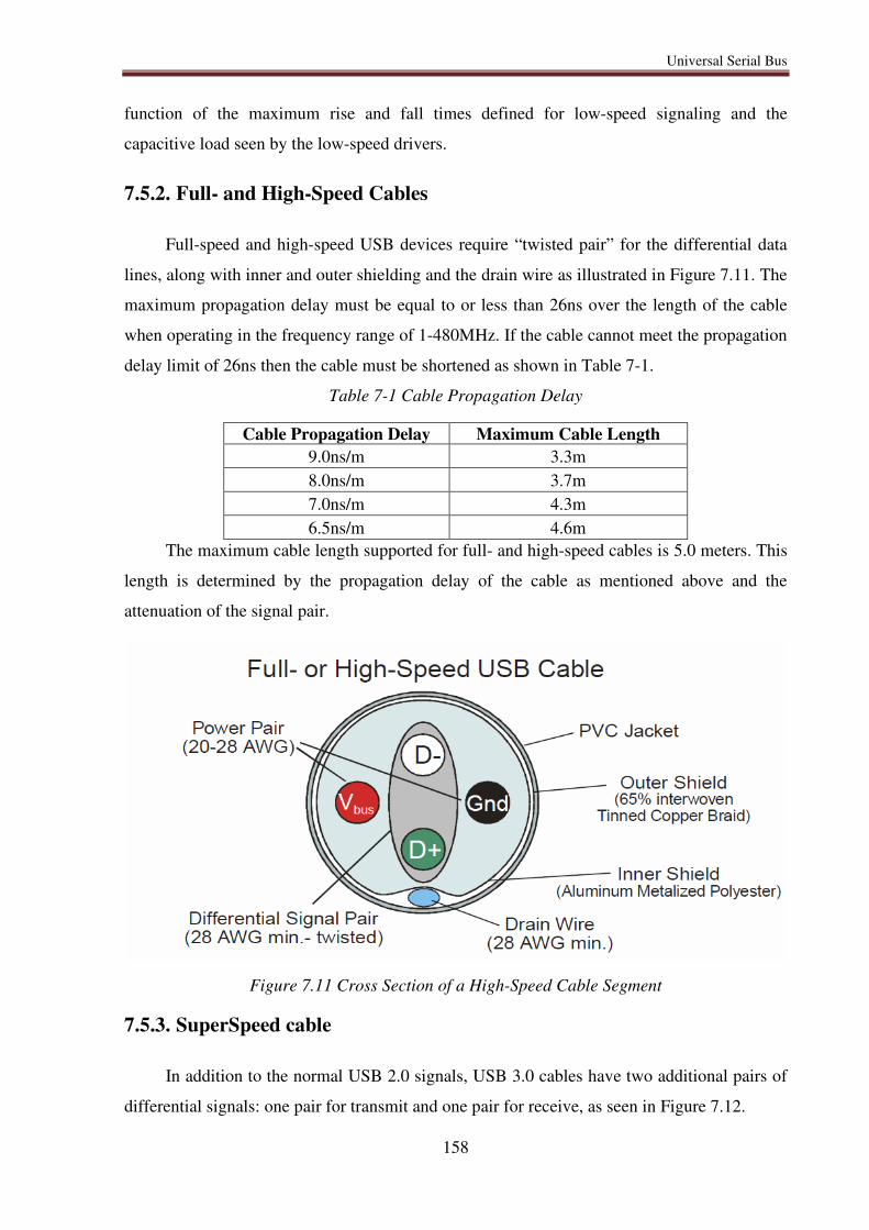
Universal Serial Bus
158
function of the maximum rise and fall times defined for low-speed signaling and the
capacitive load seen by the low-speed drivers.
7.5.2. Full- and High-Speed Cables
Full-speed and high-speed USB devices require “twisted pair” for the differential data
lines, along with inner and outer shielding and the drain wire as illustrated in Figure 7.11. The
maximum propagation delay must be equal to or less than 26ns over the length of the cable
when operating in the frequency range of 1-480MHz. If the cable cannot meet the propagation
delay limit of 26ns then the cable must be shortened as shown in Table 7-1.
Table 7-1 Cable Propagation Delay
Cable Propagation Delay Maximum Cable Length
9.0ns/m 3.3m 8.0ns/m 3.7m 7.0ns/m 4.3m 6.5ns/m 4.6m
The maximum cable length supported for full- and high-speed cables is 5.0 meters. This
length is determined by the propagation delay of the cable as mentioned above and the
attenuation of the signal pair.
Figure 7.11 Cross Section of a High-Speed Cable Segment
7.5.3. SuperSpeed cable
In addition to the normal USB 2.0 signals, USB 3.0 cables have two additional pairs of
differential signals: one pair for transmit and one pair for receive, as seen in Figure 7.12.
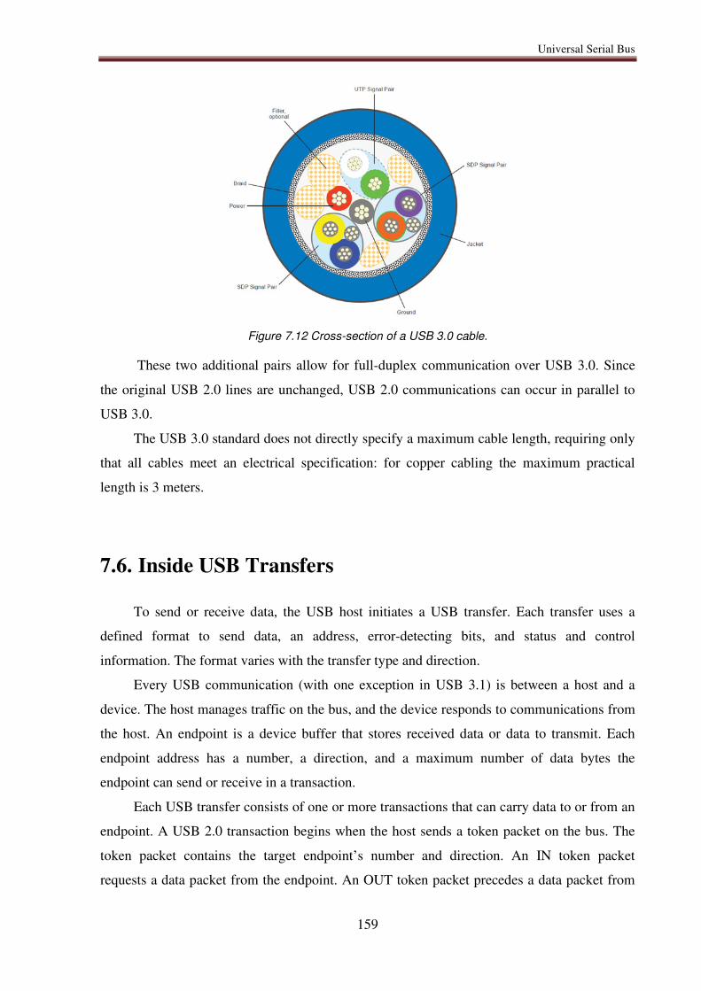
Universal Serial Bus
159
Figure 7.12 Cross-section of a USB 3.0 cable.
These two additional pairs allow for full-duplex communication over USB 3.0. Since
the original USB 2.0 lines are unchanged, USB 2.0 communications can occur in parallel to
USB 3.0.
The USB 3.0 standard does not directly specify a maximum cable length, requiring only
that all cables meet an electrical specification: for copper cabling the maximum practical
length is 3 meters.
7.6. Inside USB Transfers
To send or receive data, the USB host initiates a USB transfer. Each transfer uses a
defined format to send data, an address, error-detecting bits, and status and control
information. The format varies with the transfer type and direction.
Every USB communication (with one exception in USB 3.1) is between a host and a
device. The host manages traffic on the bus, and the device responds to communications from
the host. An endpoint is a device buffer that stores received data or data to transmit. Each
endpoint address has a number, a direction, and a maximum number of data bytes the
endpoint can send or receive in a transaction.
Each USB transfer consists of one or more transactions that can carry data to or from an
endpoint. A USB 2.0 transaction begins when the host sends a token packet on the bus. The
token packet contains the target endpoint’s number and direction. An IN token packet
requests a data packet from the endpoint. An OUT token packet precedes a data packet from
Universal Serial Bus
160
the host. In addition to data, each data packet contains error-checking bits and a Packet ID
(PID) with a data-sequencing value. Many transactions also have a handshake packet where
the receiver of the data reports success or failure of the transaction.
For Enhanced SuperSpeed transactions, the packet types and protocols differ, but the
transactions contain similar addressing, error-checking, and data-sequencing values along
with the data.
USB supports four transfer types: control, bulk, interrupt, and isochronous. In a
control transfer, the host sends a defined request to the device. On device attachment, the host
uses control transfers to request a series of data structures called descriptors from the device.
The descriptors provide information about the device’s capabilities and help the host decide
what driver to assign to the device. A class specification or vendor can also define requests.
Control transfers have up to three stages: Setup, Data (optional), and Status. The Setup
stage contains the request. When present, the Data stage contains data from the host or device,
depending on the request. The Status stage contains information about the success of the
transfer. In a control read transfer, the device sends data in the Data stage. In a control write
transfer, the host sends data in the Data stage, or the Data stage is absent.
The other transfer types don’t have defined stages. Instead, higher-level software
defines how to interpret the raw data. Bulk transfers are intended for applications where the
rate of transfer isn’t critical, such as sending a file to a printer or accessing files on a drive.
For these applications, quick transfers are nice, but the data can wait if necessary. On a busy
bus, bulk transfers have to wait, but on a bus that is otherwise idle, bulk transfers are the
fastest. Low speed devices don’t support bulk transfer.
Interrupt transfers are for devices that must receive the host’s or device’s attention
periodically, or with low latency, or delay. Other than control transfers, interrupt transfers are
the only way low-speed devices can transfer data. Keyboards and mice use interrupt transfers
to send keypress and mouse-movement data. Interrupt transfers can use any speed.
Isochronous transfers have guaranteed delivery time but no error correcting. Data that
uses isochronous transfers includes streaming audio and video. Isochronous is the only
transfer type that doesn’t support automatic re-transmitting of data received with errors, so
occasional errors must be acceptable. Low-speed devices don’t support isochronous transfer
Universal Serial Bus
161
7.6.1. Managing data on the bus
The host schedules the transfers on the bus. A USB 2.0 host controller manages traffic
by dividing time into 1-ms frames at low and full speeds and 125-μs microframes at high
speed. The host allocates a portion of each (micro)frame to each transfer. Each (micro)frame
begins with a Start-of-Frame (SOF) timing reference.
An Enhanced SuperSpeed bus doesn’t use SOFs, but the host schedules transfers within
125-μs bus intervals. A USB 3.1 host also sends timestamp packets once every bus interval to
all Enhanced SuperSpeed ports that aren’t in a low-power state.
Each transfer consists of one or more transactions. Control transfers always have
multiple transactions because they have multiple stages, each consisting of one or more
transactions. Other transfer types use multiple transactions when they have more data than
will fit in a single transaction. Depending on how the host schedules the transactions and the
speed of a device’s response, the transactions in a transfer may all be in a single (micro)frame
or bus interval, or the transactions may be spread over multiple (micro)frames or bus
intervals.
Every device has a unique address assigned by the host, and all data travels to or from
the host. Except for remote wakeup signaling, everything a USB 2.0 device sends is in
response to receiving a packet sent by the host. Because multiple devices can share a data path
on the bus, each USB 2.0 transaction includes a device address that identifies the transaction’s
destination.
Enhanced SuperSpeed devices can send status and control information to the host
without waiting for the host to request the information. Every Enhanced SuperSpeed Data
Packet and Transaction Packet includes a device address. Enhanced SuperSpeed buses also
use Link Management Packets that travel only between a device and the nearest hub and thus
don’t need addressing information.
7.6.2. Elements of a transfer
Every USB transfer consists of one or more transactions, and each transaction in turn
contains packets of information. To understand transactions, packets, and their contents, you
also need to understand endpoints and pipes.
Universal Serial Bus
162
Endpoints: the source and sink of data
All bus traffic travels to or from a device endpoint. The endpoint is a buffer that
typically stores multiple bytes and consists of a block of data memory or a register in the
device-controller chip. The data stored at an endpoint may be received data or data waiting to
transmit. The host also has buffers that hold received data and data waiting to transmit, but the
host doesn’t have endpoints. Instead, the host serves as the source and destination for
communicating with device endpoints.
An endpoint address consists of an endpoint number and direction. The number is a
value in the range 0–15. The direction is defined from the host’s perspective: an IN endpoint
provides data to send to the host and an OUT endpoint stores data received from the host. An
endpoint configured for control transfers must transfer data in both directions so a control
endpoint consists of a pair of IN and OUT endpoint addresses that share an endpoint number.
Every device must have endpoint zero configured as a control endpoint. Additional
control endpoints offer no improvement in performance and thus are rare.
In other transfer types, the data flows in one direction though status and control
information can travel in the opposite direction. A single endpoint number can support both
IN and OUT endpoint addresses. For example, a device might have endpoint 1 IN for sending
data to the host and endpoint 1 OUT for receiving data from the host.
In addition to endpoint zero, a full- or high-speed device can have up to 30 additional
endpoint addresses (1–15, IN and OUT). A low-speed device can have at most two additional
endpoint addresses which can be two IN, two OUT, or one in each direction.
Pipes: connecting endpoints to the host
Before data can transfer, the host and device must establish a pipe. A pipe is an
association between a device’s endpoint and the host controller’s software. Host software
establishes a pipe with each endpoint address the host wants to communicate with.
The host establishes pipes during enumeration. If a user detaches a device from the bus,
the host removes the no longer needed pipes. The host can also request new pipes or remove
unneeded pipes by using control transfers to request an alternate configuration or interface for
a device. Every device has a default control pipe that uses endpoint zero.
The configuration information received by the host includes an endpoint descriptor for
each endpoint the device wants to use. Each endpoint descriptor contains an endpoint address,
the type of transfer the endpoint supports, the maximum size of data packets, and, for
Universal Serial Bus
163
interrupt and isochronous transfers, the desired service interval, or period of time between
attempts to send or receive data.
7.6.3. Transaction types
Every USB 2.0 transaction begins with a packet that contains an endpoint number and a
code that indicates the direction of data flow and whether the transaction is initiating a control
transfer:
Transaction
Type
Source of
Data
Types of Transfers that Use the
Transaction Type
Contents
IN device all data or status information
OUT host all data or status information
Setup host control a request
As with endpoint directions, the naming convention for IN and OUT transactions is
from the perspective of the host. In an IN transaction, data travels from the device to the host.
In an OUT transaction, data travels from the host to the device.
A Setup transaction is like an OUT transaction because data travels from the host to the
device, but a Setup transaction is a special case because it initiates a control transfer. Devices
need to identify Setup transactions because these are the only transactions that devices must
always accept. Any transfer type may use IN or OUT transactions.
In every USB 2.0 transaction, the host sends an addressing triple that consists of a
device address, an endpoint number, and endpoint direction. On receiving an OUT or Setup
packet, the endpoint stores the data that follows the packet, and the device hardware typically
triggers an interrupt. Firmware can then process the received data and take any other required
action. On receiving an IN packet, if the endpoint has data ready to send to the host, the
hardware sends the data on the bus and typically triggers an interrupt. Firmware can then do
whatever is needed to get ready to send data in the next IN transaction. An endpoint that isn’t
ready to send or receive data in response to an IN or OUT packet sends a status code.
7.6.4. USB 2.0 transfers
Figure 7.13 shows the elements of a typical USB 2.0 transfer. A lot of the terminology
here begins to sound the same. There are transfers and transactions, stages and phases, data
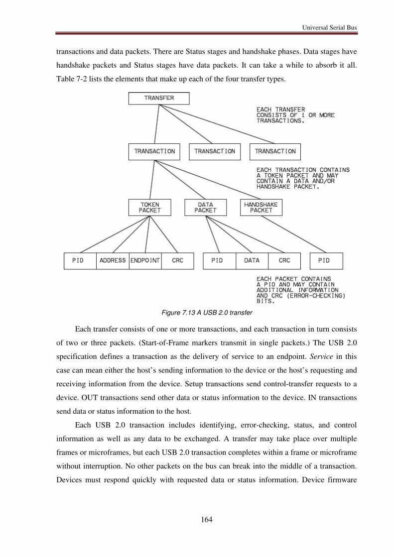
Universal Serial Bus
164
transactions and data packets. There are Status stages and handshake phases. Data stages have
handshake packets and Status stages have data packets. It can take a while to absorb it all.
Table 7-2 lists the elements that make up each of the four transfer types.
Figure 7.13 A USB 2.0 transfer
Each transfer consists of one or more transactions, and each transaction in turn consists
of two or three packets. (Start-of-Frame markers transmit in single packets.) The USB 2.0
specification defines a transaction as the delivery of service to an endpoint. Service in this
case can mean either the host’s sending information to the device or the host’s requesting and
receiving information from the device. Setup transactions send control-transfer requests to a
device. OUT transactions send other data or status information to the device. IN transactions
send data or status information to the host.
Each USB 2.0 transaction includes identifying, error-checking, status, and control
information as well as any data to be exchanged. A transfer may take place over multiple
frames or microframes, but each USB 2.0 transaction completes within a frame or microframe
without interruption. No other packets on the bus can break into the middle of a transaction.
Devices must respond quickly with requested data or status information. Device firmware
Universal Serial Bus
165
typically arms, or sets up, an endpoint’s response to a received packet, and on receiving a
packet, the hardware places the response on the bus.
Table 7-2 Transactions in USB2.0 transfers
Transfer Type
Number and Direction of Transactions Phases (packets)
Control Setup Stage
1 (SETUP) Token Data Handshake
Data Stage
Zero or more (IN or OUT)
Token Data Handshake
Status Stage
1 (opposite direction of the transaction(s) in the Data stage or IN if there is no Data stage)
Token Data Handshake
Bulk 1 or more (IN or OUT)
Token Data Handshake
Interrupt 1 or more (IN or OUT)
Token Data Handshake
Isochronous 1 or more (IN or OUT)
Token Data
A non-control transfer with a small amount of data may complete in a single
transaction. Other transfers use multiple transactions with each carrying a portion of the data.
Transaction phases
Each transaction has up to three phases, or parts that occur in sequence: token, data, and
handshake. Each phase consists of one or two transmitted packets. Each packet is a block of
information with a defined format. All packets begin with a Packet ID (PID) that contains
identifying information (Table 7-3). Depending on the transaction, the PID may be followed
by an endpoint address, data, status information, or a frame number, along with error-
checking bits.
In the token phase of a transaction, the host initiates a communication by sending a
token packet. The PID indicates the transaction type, such as Setup, IN, OUT, or SOF.
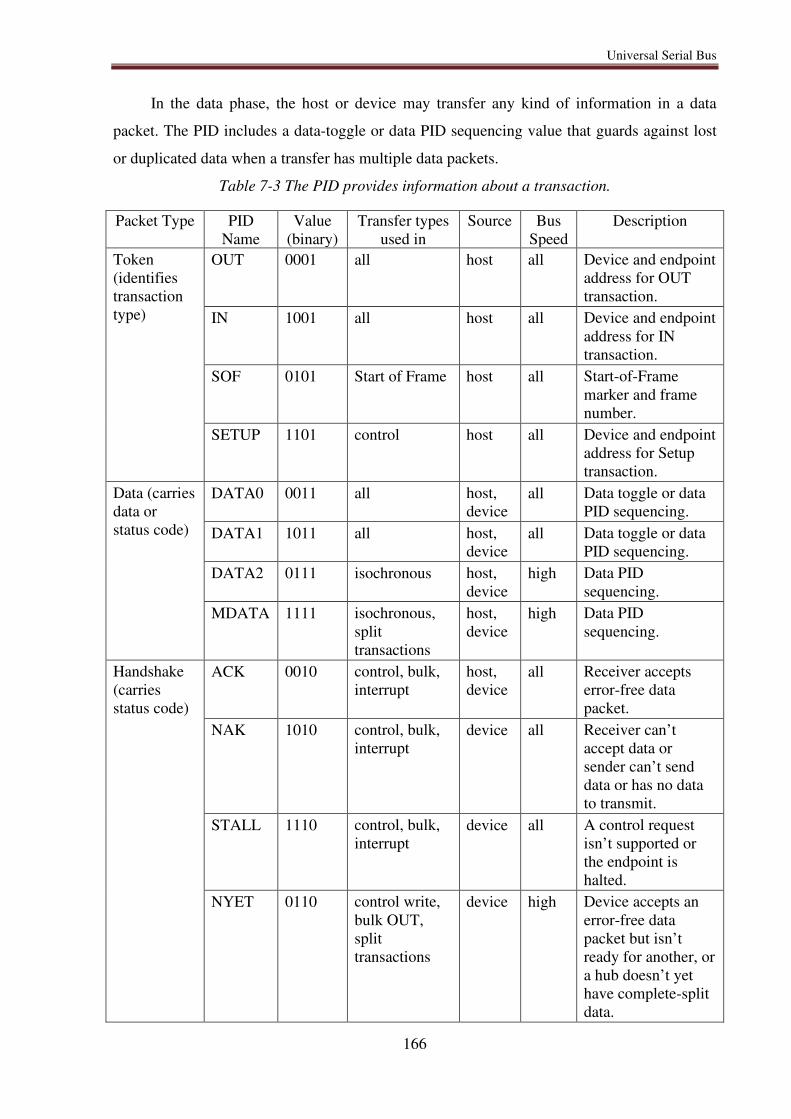
Universal Serial Bus
166
In the data phase, the host or device may transfer any kind of information in a data
packet. The PID includes a data-toggle or data PID sequencing value that guards against lost
or duplicated data when a transfer has multiple data packets.
Table 7-3 The PID provides information about a transaction.
Packet Type PID Name
Value (binary)
Transfer types used in
Source Bus Speed
Description
Token (identifies transaction type)
OUT 0001 all host all Device and endpoint address for OUT transaction.
IN 1001 all host all Device and endpoint address for IN transaction.
SOF 0101 Start of Frame host all Start-of-Frame marker and frame number.
SETUP 1101 control host all Device and endpoint address for Setup transaction.
Data (carries data or status code)
DATA0 0011 all host, device
all Data toggle or data PID sequencing.
DATA1 1011 all host, device
all Data toggle or data PID sequencing.
DATA2 0111 isochronous host, device
high Data PID sequencing.
MDATA 1111 isochronous, split transactions
host, device
high Data PID sequencing.
Handshake (carries status code)
ACK 0010 control, bulk, interrupt
host, device
all Receiver accepts error-free data packet.
NAK 1010 control, bulk, interrupt
device all Receiver can’t accept data or sender can’t send data or has no data to transmit.
STALL 1110 control, bulk, interrupt
device all A control request isn’t supported or the endpoint is halted.
NYET 0110 control write, bulk OUT, split transactions
device high Device accepts an error-free data packet but isn’t ready for another, or a hub doesn’t yet have complete-split data.
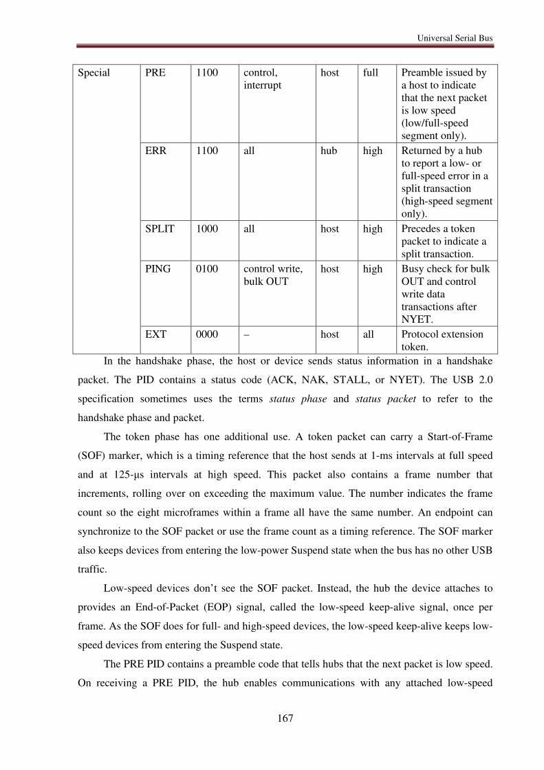
Universal Serial Bus
167
Special PRE 1100 control, interrupt
host full Preamble issued by a host to indicate that the next packet is low speed (low/full-speed segment only).
ERR 1100 all hub high Returned by a hub to report a low- or full-speed error in a split transaction (high-speed segment only).
SPLIT 1000 all host high Precedes a token packet to indicate a split transaction.
PING 0100 control write, bulk OUT
host high Busy check for bulk OUT and control write data transactions after NYET.
EXT 0000 – host all Protocol extension token.
In the handshake phase, the host or device sends status information in a handshake
packet. The PID contains a status code (ACK, NAK, STALL, or NYET). The USB 2.0
specification sometimes uses the terms status phase and status packet to refer to the
handshake phase and packet.
The token phase has one additional use. A token packet can carry a Start-of-Frame
(SOF) marker, which is a timing reference that the host sends at 1-ms intervals at full speed
and at 125-μs intervals at high speed. This packet also contains a frame number that
increments, rolling over on exceeding the maximum value. The number indicates the frame
count so the eight microframes within a frame all have the same number. An endpoint can
synchronize to the SOF packet or use the frame count as a timing reference. The SOF marker
also keeps devices from entering the low-power Suspend state when the bus has no other USB
traffic.
Low-speed devices don’t see the SOF packet. Instead, the hub the device attaches to
provides an End-of-Packet (EOP) signal, called the low-speed keep-alive signal, once per
frame. As the SOF does for full- and high-speed devices, the low-speed keep-alive keeps low-
speed devices from entering the Suspend state.
The PRE PID contains a preamble code that tells hubs that the next packet is low speed.
On receiving a PRE PID, the hub enables communications with any attached low-speed
Universal Serial Bus
168
devices. On a low- and full-speed bus, the PRE PID precedes all token, data, and handshake
packets directed to low-speed devices. High-speed buses encode the PRE in the SPLIT
packet, rather than sending the PRE separately. Low-speed packets sent by a device don’t
require a PRE PID.
In a high-speed bulk or control transfer with multiple data packets, before sending the
second and any subsequent data packets, the host may send a PING PID to find out if the
endpoint is ready to receive more data. The device responds with a status code.
The SPLIT PID identifies a token packet as part of a split. The ERR PID is only for split
transactions to enable a USB 2.0 hub to report an error in a downstream low- or full-speed
transaction. The ERR and PRE PIDs have the same value but don’t cause confusion because a
hub never sends a PRE to the host or an ERR to a device. Also, ERR is only for high-speed
segments and PRE never transmits on high-speed segments.
7.6.5. SuperSpeed transfers
Like USB 2.0, SuperSpeed buses carry data, addressing, and status and control
information. But SuperSpeed has a dedicated data path for each direction, more support for
power conservation, and other enhancements for greater efficiency. To support these
differences, SuperSpeed transactions use different packet formats and protocols.
Packet types
SuperSpeed communications use two packet types when transferring data:
A Transaction Packet (TP) carries status and control information.
A Data Packet (DP) carries data and status and control information.
Two additional packet types perform other functions:
An Isochronous Timestamp Packet (ITP) carries timing information that devices can use
for synchronization. The host multicasts an ITP following each bus-interval boundary to
all links that aren’t in a low-power state. The timestamp holds a count from zero to
0x3FFF and rolls over on overflow.
A Link Management Packet (LMP) travels only in the link between a device’s port and
the hub the device connects to. The ports are called link partners. LMPs help manage
the link.
Enhanced SuperSpeed doesn’t use token packets because packet headers contain the
token packet’s information. Instead of data toggles, SuperSpeed uses 5-bit sequence numbers
that roll over from 31 to zero.
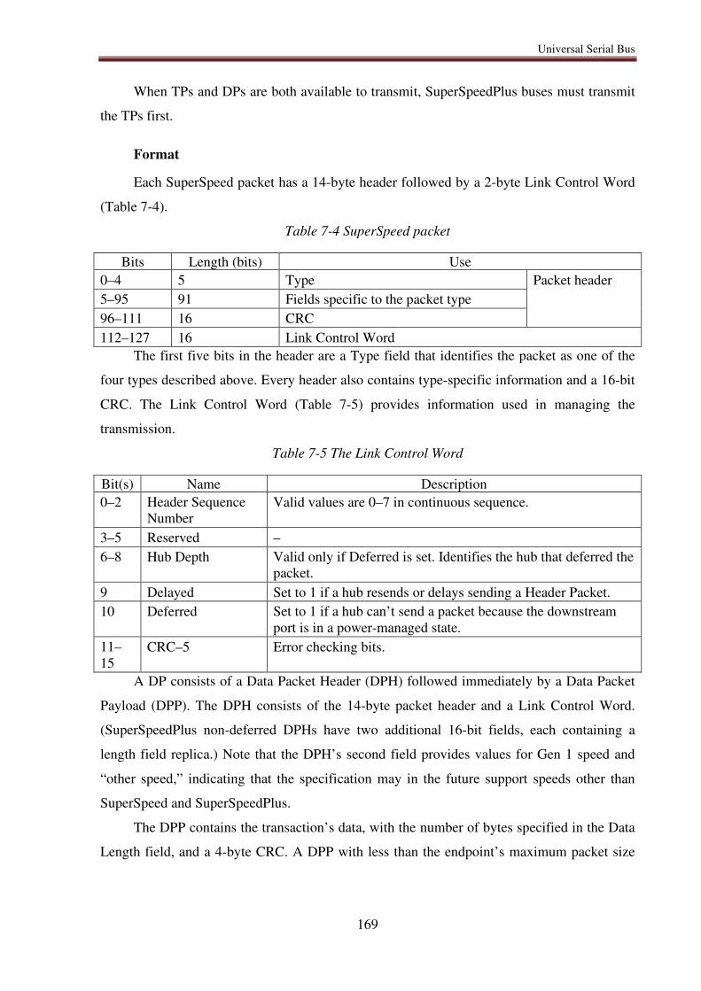
Universal Serial Bus
169
When TPs and DPs are both available to transmit, SuperSpeedPlus buses must transmit
the TPs first.
Format
Each SuperSpeed packet has a 14-byte header followed by a 2-byte Link Control Word
(Table 7-4).
Table 7-4 SuperSpeed packet
Bits Length (bits) Use
0–4 5 Type Packet header 5–95 91 Fields specific to the packet type 96–111 16 CRC 112–127 16 Link Control Word
The first five bits in the header are a Type field that identifies the packet as one of the
four types described above. Every header also contains type-specific information and a 16-bit
CRC. The Link Control Word (Table 7-5) provides information used in managing the
transmission.
Table 7-5 The Link Control Word
Bit(s) Name Description
0–2 Header Sequence Number
Valid values are 0–7 in continuous sequence.
3–5 Reserved – 6–8 Hub Depth Valid only if Deferred is set. Identifies the hub that deferred the
packet. 9 Delayed Set to 1 if a hub resends or delays sending a Header Packet. 10 Deferred Set to 1 if a hub can’t send a packet because the downstream
port is in a power-managed state. 11–15
CRC–5 Error checking bits.
A DP consists of a Data Packet Header (DPH) followed immediately by a Data Packet
Payload (DPP). The DPH consists of the 14-byte packet header and a Link Control Word.
(SuperSpeedPlus non-deferred DPHs have two additional 16-bit fields, each containing a
length field replica.) Note that the DPH’s second field provides values for Gen 1 speed and
“other speed,” indicating that the specification may in the future support speeds other than
SuperSpeed and SuperSpeedPlus.
The DPP contains the transaction’s data, with the number of bytes specified in the Data
Length field, and a 4-byte CRC. A DPP with less than the endpoint’s maximum packet size
Universal Serial Bus
170
bytes is a short packet. A DPP consisting of just the CRC and no data is a zero-length Data
Payload.
For SuperSpeedPlus only, the DP specifies the transfer type, and non-periodic DPs
specify an arbitration rate for use by the hub in scheduling SuperSpeedPlus traffic.
The other three packet types are always 128 bytes. In a TP, the Subtype field indicates
the transaction’s purpose. All TPs have a device address that indicates the source or
destination of the packet. All TPs sent by the host contain a Route String that hubs use in
routing the packet to its destination.


